Tool Options When Debugging an FPGA-based PCIe Non-Transparent Bridge (PCIe NTB) Used in an ECU for Autonomous Driving
We share our findings and experiences when debugging an FPGA-based PCIe Non-Transparent Bridge (PCIe NTB) used in an Electronic Control Unit (ECU) for Autonomous Vehicles. After explaining key inner workings of PCIe and PCIe Non-Transparent Bridge we discuss debugging using embedded logic analyzers (Xilinx ChipScope / ILA), RTL Simulators (XSim from the Xilinx Vivado toolsuite as well as Questa Prime from Mentor Graphics) plus Visualizer, also from Mentor Graphics. We hope that you find this useful when you are preparing to debug your next FPGA project.
- Tool Options When Debugging an FPGA-based PCIe Non-Transparent Bridge (PCIe NTB) Used in an ECU for Autonomous Driving
Copyright © 2025 Missing Link Electronics. All rights reserved. Missing Link Electronics, the stylized Missing Link Electronics MLE logo are the service mark and/or trademark of Missing Link Electronics, Inc. All other product or service names and trademarks are the property of their respective owners.
1. Motivation and Outline
An Electronic Control Unit (ECU) suitable for Autonomous Driving, or better Automated Driving, requires massive compute performance to deal with the large amounts of streaming sensor data. A typical use case involves 10 or more cameras plus multiple Lidar and multiple Radar sensors. This quickly adds up to a data stream of multiple tens of Gigabits per second. Processing involves classical image processing algorithms (for example, Edge Detection) as well as DNNs (Deep Neural Networks) like Semantic Segmentation or Object Recognition. Together with the requirement to compute an action predictably within a few microseconds, most engineering teams combine multiple processing devices, CPUs, GPUs, FPGAs, from multiple vendors to tackle this compute problem. When we say CPUs or GPUs or FPGAs we actually think of the various System-on-Chip (SoC) embedded multiple CPU cores or high-performance GPU cores or Programmable Logic fabric.
PCIe is the most promising fabric to connect those CPUs and GPUs and FPGAs (short processors) to form a reliable high-bandwidth, low-latency network within a single ECU. Various options exist here. At MLE, we have been utilizing a technology called PCIe Non-Transparent Bridge (PCIe NTB). Implemented within a single automotive-grade FPGA, the Xilinx Zynq UltraScale+ MPSoC, not only can we connect multiple CPUs and GPUs and FPGAs via PCIe, but we can also offer flexible interface standards to the various sensors. And, most importantly, the use of an FPGA in the datapath between sensors and processors enables Data-in-Motion preprocessing. This so-called DADP (Data Acquisition and Data Preprocessing) allows to resample and adjust the incoming streaming sensor data, for example in terms of granularity, to make more efficient use of the CPU or GPU or FPGA architecture in charge of running the decision making algorithms down-stream.
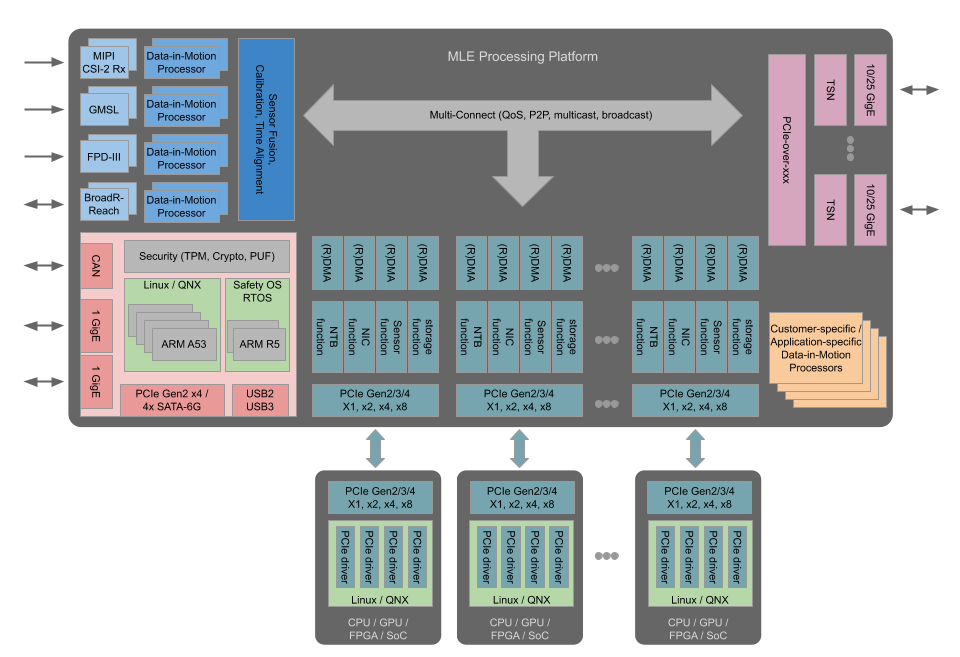
Figure 1: MLE Processing Platform for Level-4 Autonomous Driving
Debugging systems like this can be quite a challenge: PCIe as a hardware / software interface means that the problem can lie in the device driver software or in programmable logic hardware, or both. Multiple CPUs each running a rich operating system like Linux (including ROS or AUTOSAR Adaptive) tend to drive the system into unanticipated corner cases which are hard to verify upfront at module level.
Within this document we share with you some tricks and experiences when debugging. The example used throughout this document is MLE’s PCIe Non-Transparent Bridge (PCIe NTB). As tool options for debugging we discuss:
- ILA (formerly known as ChipScope) from the Xilinx Vivado toolsuite
- XSim, the RTL simulator from the Xilinx Vivado toolsuite
- Questa Prime from Mentor Graphics
- Visualizer, also from Mentor Graphics
This document is organized as follows: First, we give an introduction into the workings of PCIe – from a software engineers point-of-view as well as from an FPGA designer’s. Then we will explain PCIe Non-Transparent Bridge (PCIe NTB) – as a means to connect multiple processors via PCIe. After that we will dive into a debugging scenario when integrating PCIe NTB. We will discuss the pros & cons of the various debugger options (ILA, XSim, Questa, Visualizer) and give to you some metrics that may help you in selecting an efficient debug option. We will finish by sharing our experiences with Mentor Graphics’ (not so) new tool, Visualizer.
Enjoy reading!
2. The Workings of PCI Express (PCIe)
The Peripheral Component Interconnect Express (PCIe) standard currently in its fourth generation (Gen4) is an I/O interconnect technology defined by PCI-SIG. It is a layer based protocol that for software is fully backwards compatible to the PCI Local Bus standard which is replaced by PCIe.
The physical layer is separated into a logical and an electrical block. The electrical block defines a full-duplex high speed serial point-to-point connection with scalable link width at 1 to 32 lanes and line rates at 2.5 GT/s, 5.0 GT/s, 8.0 GT/s, . The logical block builds the PCIe frame and does the Byte stripping on multiple lanes, the serialization and the 128b/130b line encoding (Gen3).
The Data Link layer on top ensures the data integrity by the ACK/NAK semantic and Flow Control Credits. A CRC and sequence number is added to a Data Link Layer Packet (DLLP) before the transport and the DLLP is kept in the output buffer until an acknowledgment is received.
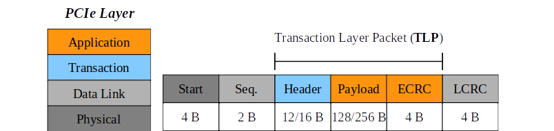
The Transaction Layer builds a TLP that is a packet from the category memory, I/O, configuration or message. Beside the transport of the application’s payload data in a memory or I/O transaction, Interrupts and PCI configuration data is delivered inside a TLP as well. The maximum payload data that is transported with one TLP is determined by the system and will mostly be 128 B or 256 B.
The PCIe topology is hierarchical. The CPU is connected to the Root Complex (RC), which generates the PCIe transactions on behalf of the processor. The RC is integrated into the CPU in modern systems. I/O devices implement a PCIe Endpoint (EP) and are connected to the RC directly or via switches. The switch consists of one Upstream Port (UP) and one or more Downstream Ports (DP). Each device in the PCIe topology is identified by an ID-tripel of Bus/Device/Function number, as well as a region in the CPU address-space.
Inside a PCIe switch, the packets are routed between the switch ports on the Transaction layer by their TLP header information. There are three different routing mechanisms: Routing by ID for configuration and completion TLPs, by address for memory- and I/O-requests and the implicit routing for messages to all downstream ports.
PCIe has posted and non-posted transactions. A non-posted transaction requires a completion TLP to be sent from the receiver back to the requester. E.g. a memory-read TLP sent by the RC, requests data from an EP. The EP answers with a completion TLP with the requested data appended. PCIe devices may also operate as bus masters for DMA transactions.
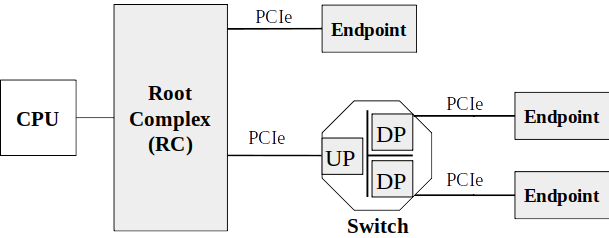
PCIe replaces the PCI Local Bus (PCI) and from a software point of view is fully backwards compatible to it. This was done by keeping the interface to software from PCI. This means that the addressing of devices, the driver model and the configuration of devices is PCI compliant. E.g. a switch consists of one upstream port and one or more downstream ports, but from a PCI point of view each switch port is a PCI-PCI-Bridge that connects the bridge primary bus with the secondary bus. A link between two PCIe devices is denoted as bus from PCI view but is still a point-to-point connection.
At the beginning of the system’s boot-up process, the device topology is unknown. The RC sends Configuration-TLPs that have to be responded to by the devices with Completion-TLPs. The Configuration-TLPs contain, amongst other things, the bus/device/function number a device needs to store in its registers.
Each PCIe device implements a set of registers, called configuration space. PCIe devices have a PCI configuration space and in addition an extended configuration space for PCIe specific capabilities. This configuration space contains registers for e.g. the device id, bus/device/function number and a register to enable bus mastering for DMA. The configuration space contains also the base address registers (BARs) for memory space and I/O space.
3. PCIe Non-Transparent Bridge (PCIe NTB) to Connect Multiple CPUs, GPUs & FPGAs
NTB stands for Non-Transparent Bridge. Unlike in a PCIe (transparent) Bridge where the RC “sees” all the PCIe busses all the way to all the Endpoints, an NTB forwards the PCIe traffic between the separate PCIe busses like a bridge. Each RC sees the NTB as an Endpoint device but does not see the other RC and devices on the other side. Means, everything behind the NTB is not directly visible to the particular RC, thus “Non-Transparent”.
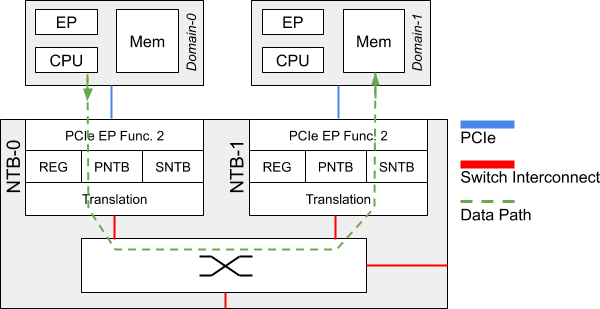
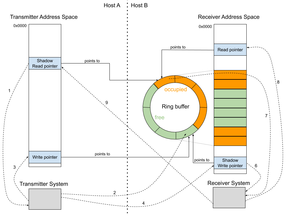
For each attached RC there is a memory aperture allocated to the NTB within the main memory of said RC. PCIe writes (and reads) are translated across. Given the nature of PCIe so-called Posted Writes, writing data into a remote RC’s main memory carries less overhead than reading data from a remote RC’s main memory. Therefore, at MLE for sending data from one RC to a second RC we fully use this concept of Posted Writes together with so-called Doorbell Registers to implement a very efficient and high-performance communication mechanism. Groundwork for this was laid more than a decade ago by work from Jack Regula and others . Figure 6 shows this communication mechanism across an NTB based on a ring buffer structure for the example of two RCs, Host A and Host B.
As NTB has been enjoying support in the Open Source Linux kernel we do adhere to this de facto standard API described in Linux ntb.h and made our programmable logic implementation compatible to it.
Unlike in Datacenter applications with their wide PCIe busses of 16 or 32 lanes (or even more) in an automotive ECU you have to be frugal with those high-speed IO lanes. This means that we cannot use the Daisy Chain connectivity scheme for connecting multiple RCs (means three or more) which is, for example, described in “Intel Xeon Processor C5500/C3500 Series Non-Transparent Bridge”: When using four, or less, PCIe lanes to connect, traffic would quickly saturate the PCIe links of the RCs on the “inside” of the Daisy Chain. Therefore at MLE we have implemented a Peer-to-Peer connectivity scheme which, by the way, can be done quite efficiently in an FPGA in terms of resources and performance when using Xilinx AXI4 network-on-chip infrastructure. This Peer-to-Peer connectivity scheme avoids lookup tables for translating between sender and receiver PCIe Device IDs, something that has to be done using the Daisy Chain approach.
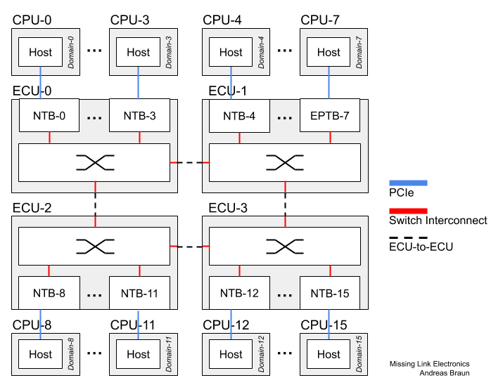
And, we can also extend connectivity to more than 32 RCs (the PCIe Device ID field is only 5 bits) without any extra measures which would add to the overall communication latency. This enables you to build a system-of-systems, for example by connecting multiple ECUs via automotive high-speed Ethernet (10G or soon 25G) as shown in Figure 7 where all 16 CPUs can directly exchange data with all other 15 CPUs via PCIe.
Furthermore, one of the key reasons of using multiple CPUs or GPUs or FPGAs in an automotive application is resilience to hardware failures to deliver a high level of functional safety according to DIN/ISO 61508 or DIN/ISO 26262. This is why we have added certain checks into MLE’s NTB technology.
The PNTB (Primary NTB) which is in charge of egress PCIe traffic, besides other checks, on-the-fly validates address ranges – easy to do in a Xilinx FPGA – to prevent that a software on the sending RC sends data from memory spaces other than the memory space pre-registered for NTB communication. Similarly, the SNTB (Secondary NTB) which is in charge of ingress PCIe traffic checks that communication writes only into valid address spaces. In combination, this also allows us to maintain a reliable communication even if a SEU (Single Event Upset) might have flipped an address bit. Further checks allow to detect malfunction of any RC and to respond to it by rerouting the PCIe traffic to a backup RC.
With all these measure it made implementing MLE’s NTB technology quite a challenge – and this is why we looked closely into good tools for FPGA system debugging.
4. Tool Options for FPGA Debugging in PCIe NTB
Throughout the rest of this paper we will be looking into FPGA debugging. We start with a description of our simulation setup including testbench and DUT/UUT, then compare some aspects of key debugging tools such as
- Xilinx ILA (formerly known as ChipScope),
- Xilinx RTL simulator, XSim,
- Questa Prime from Mentor Graphics,
and then focus on debugging using RTL simulation plus a powerful debugger front-end called Visualizer.
FPGA debugging is quite different from software debugging (with GDB, for example). However, because of the rich software aspects of PCIe it is not just RTL debugging either. The example we are using is a “bug” within our NTB block written in Verilog HDL that is difficult to uncover using RTL module-level simulation. This bug causes wrong processing of the address in the TLB within the NTB block. The symptom is that certain PCIe Requests got lost on their path from sender interface (A) to receiver interface (B) (see Figure 8).
4.1 System-Level Simulation of PCIe NTB – PHY or PIPE?
Figure 8 shows this system-level setup which is quite typical – and very effective – in verifying / debugging PCIe based hardware/software systems.
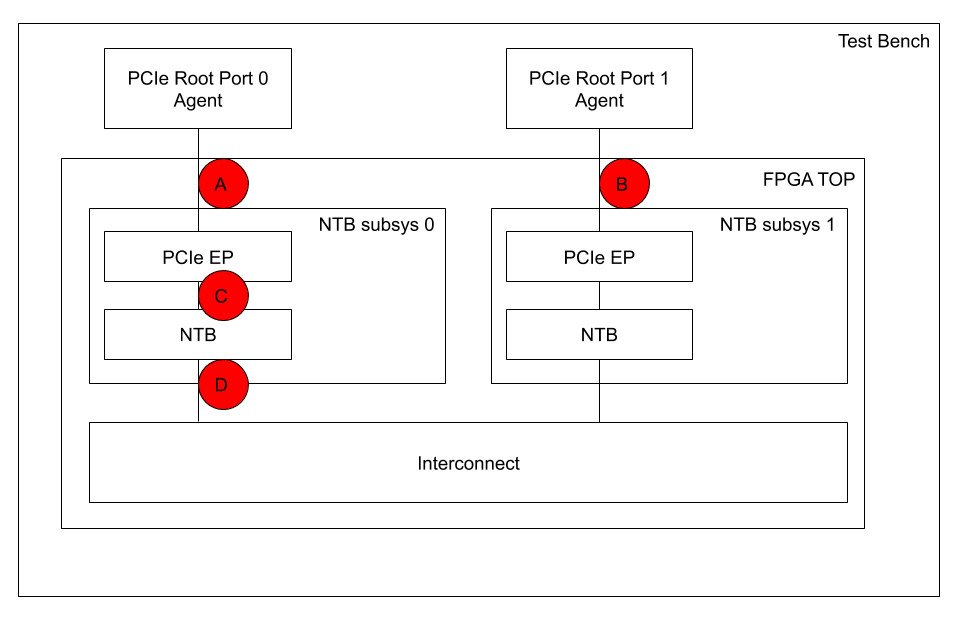
The Testbench instantiates our FPGA TOP Module which comprises two separate instances of an NTB subsystem, NTB subsys 0 and NTB subsys 1, each of which is our NTB block connected to a PCIe EP (Endpoint) instance from the Xilinx IP library. Both NTB subsystems are connected through an Interconnect, implementing a so-called Back-to-Back connection. The Testbench further comprises two instances of a PCIe Root Port Agent (RPA), PCIe Root Port 0 Agent (RPA0) and PCIe Root Port 1 Agent (RPA1), each of which is connected to their respective PCIe EP via connection (A), and (B). These agents perform both, generating PCIe transactions for stimuli as well as checking the responses. Built on top of those agents we have implemented scripts that perform almost a complete run through the startup process of PCIe – including the distinct steps of PCIe Enumeration, PCIe EP Configuration and PCIe NTB Configuration. Simulation finishes with data transfers between the two hosts by performing PCIe Posted Write transactions which emulate the software. See above for details of the inner workings of PCIe.
In our verification approach we are using two concepts for connecting these agents with the NTB subsystems – connections at Point (A) and Point (B) in Figure 8: One is PHY-level the other is PIPE-level.
PHY-level simulation means you simulate PCIe at the level of a Multi-Gigabit Transceiver. Xilinx provides you with a simulation model for those. The benefit of PHY-level simulation is that you run the same stream of ones and zeros as you would see when tracing the Rx / Tx SerDes IOs of the FPGA, including certain timing aspects (for example, so-called PCIe code group detection and synchronization of the PCIe symbols).
PIPE-level simulation means the PHY Interface for PCI Express (PIPE), basically one layer up from the PHY layer, excluding the PCS/PMA (analog) layers. Therefore, you cannot see PCIe symbols anymore, like in PHY-level simulation. Means, simulation has much less details and, therefore, runs much faster.
For both setups, PHY- and PIPE-level simulation we want to share with you an important metric when debugging: The time spent while waiting for the simulator to run through the test cases which is an indication for the Turn-Around-Time when interactively debugging.
Table 1 (for PIPE-level) and Table 2 (for PHY-level) present the runtimes for simulation using XSim from the Xilinx Vivado toolsuite version 2018.3, Questa Prime 2019.1 from Mentor Graphics. The latter is for Questa alone as well as for Questa when performing instrumentation to utilize the Visualizer debugger. To give you some more insight into debugging PCIe we have broken up runtime among the three steps in PCIe, Enumeration, Initialization and Data Transfer.
|
PCIe PIPE-Level |
Simulation Time [nano seconds] |
Runtime [seconds] |
||
|
PCIe Step |
XSim |
Questa |
Questa w/ Visualizer |
|
|
EP Enumeration |
161,212.0 |
1,322.0 |
57.8 |
68.8 |
|
EP Initialization |
11,348.0 |
99.0 |
6.6 |
9.3 |
|
Data Transfers |
83,604.0 |
1,154.0 |
111.2 |
138.9 |
|
Total |
256,164.0 |
2,575.0 |
175.7 |
217.0 |
Table 1: PCIe PIPE-Level Simulation Runtimes
|
PCIe PIPE-Level |
Simulation Time [nano seconds] |
Runtime [seconds] |
||
|
PCIe Step |
XSim |
Questa |
Questa w/ Visualizer |
|
|
EP Enumeration |
161,212.0 |
5,478.0 |
566.0 |
652.5 |
|
EP Initialization |
11,348.0 |
225.0 |
66.2 |
94.3 |
|
Data Transfers |
83,604.0 |
2,805.0 |
444.4 |
467.1 |
|
Total |
256,164.0 |
8,508.0 |
1,076.5 |
1,213.8 |
Table 2: PCIe PHY-Level Simulation Runtimes
Our first observation here is that XSim – while being a great, cost-efficient RTL simulator which is integrated nicely into the Xilinx Vivado toolchain – starts to “run out of steam” for such system-level PCIe simulation setups. While you wait a few minutes when running Questa, simulation runtimes for XSim can be half an hour at PIPE-level or up to several hours at PHY-level. The latter we consider as just not practical for FPGA debugging.
Our second observation is that you can reduce your turn-around-time down to one third if you are willing to give up details of PHY-level simulation in favor of the faster PIPE-level simulation. Another viewpoint would be that PHY-level simulation while giving more details is very feasible with a simulator like Questa!
4.2 FPGA Debugging with Xilinx ILA / ChipScope
Some remarks on using Xilinx ILA / ChipScope for debugging PCIe NTB:
Yes, we love Xilinx ILA / ChipScope and it is a tool regularly used from our debug bag of tricks. The ability to have design visibility into the inner workings of an FPGA is very helpful, in particular when debugging a Programmable System-on-Chip. It is nicely enhanced to also inspect the various AXI4-based network-on-chip connections we typically need.
However, in real life a PCIe-based FPGA design integrates many function blocks making the FPGA gate count (or LUT count) quite large and the compile times quite long. For example, the compile time including synthesis and place-and-route for one of our PCIe NTB implementations can take a couple of hours on a decent machine. This negatively impacts our turn-around-time.
Second, Xilinx ILA / ChipScope instantiates large monolithic blocks in an already large design (from an FPGA utilization point-of-view). With the lower FPGA speed-grade (-1) in an automotive application high clock frequencies can become a challenge for timing closure. Thus, it is quite common to instantiate 256-bit wide AXI-Streams to meet bandwidth requirements, which then requires enough Block RAM for ILA / ChipScope to sniff multiple 256-bit wide AXI-Streams. Besides longer compile times this can also cause timing violations because more logic needs to be placed and routed.
Furthermore, debugging with Xilinx ILA / ChipScope is a highly iterative approach because you do not get full design visibility. Sometimes you find out that you need to look at more signals which forces you to go back to Square One: Re-instrument and re-compile.
Overall this makes debugging with ILA / ChipScope become a Plan B, only after we cannot identify the issue in RTL simulation first.
5. Debugging with Visualizer
Recently, our partners at EDA Direct introduced us to a new RTL debugger called Visualizer. Visualizer quite nicely complements our RTL simulation approach with Questa. This section is on sharing our observations when debugging a real-life issue in our NTB block.
The symptom was that certain PCIe Requests got lost on their path from the sender interface (A) to the receiver interface (B) (see Figure 8). The root cause was that address slicing was off by one bit (thanks to a Verilog Define): In the address encoding of a Memory Write TLP (see Figure 2) the fields TLP_address[C:B] denote the so-called Partition Access Number while the fields TLP_address[B-1:0] indicate the address offset within the partition. In our implementation the width parameter B for address slicing shall be integer 24 instead of 25.
The symptom in RTL simulation was that one test case fails with an error because TLPs sent through interface (A) were never received at interface (B).
Figure 8 shows the PCIe NTB System Level Simulation Test bench, where the FPGA top level is instantiated as Unit Under Test (UUT) and the PCIe Interfaces for both NTB ports are connected to the PCIe Root Port Agents which emulate the PCIe Host. In order to locate the point where the TLPs get lost during transmission, we run the Questa simulation with Visualizer flags to generate the output database files to be used for debugging in Visualizer. We then open the database files with Visualizer and start debugging from top to bottom, beginning with the PCIe Root Port 0 Agent’s AXI-Stream Interface (A). We add the signals to the waveform view and group the AXI interfaces (A) and (B). Visualizer nicely colors the groups automatically, see Figure 9.
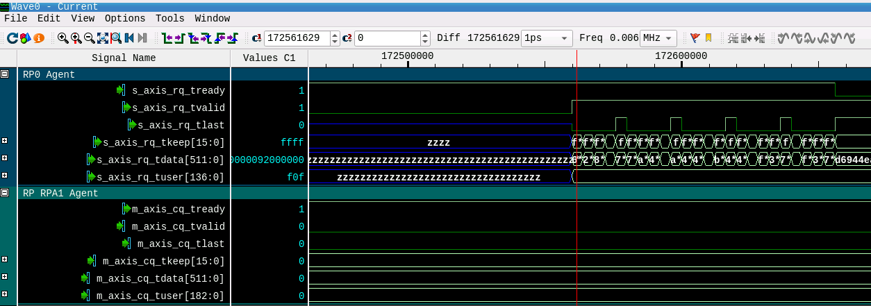
Figure 9 shows the Visualizer waveform view. The AXI-Stream Interface (A) from PCIe Root Port 0 Agent (RPA0) to UUT FPGA TOP we named RC for the Xilinx Requester Request interface. The AXI-Stream Interface (B) from UUT to PCIe Root Port 1 Agent we named CQ for the Xilinx Completer Request interface. The blue colored signal group “RPA0 Agent” with all the Requester Requests (signals named *rq* – shorthand: RQ) shows packet transfers by TLAST, TVALID and TREADY assertion which show that TLPs are transferred from the “RPA0” to the UUT. The turquoise colored signal group “RPA1 Agent” with all Completion Requests (signals named *cq* – shorthand: CQ) shows no packet transfers from the UUT to the PCIe Root Port 1 Agent. This means that the TLPs are not properly translated from the PCIe domain “RPA0” into the PCIe domain “RPA1”.
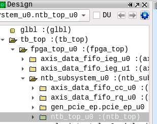
In the next step we investigate the NTB core instance ntb_top to check whether TLPs get already lost at the primary side of the NTB – indicated in Figure 8 as the path between connection (C) and connection (D). Visualizer displays the module hierarchy in the Design View of Figure 10. By expanding the folders, the instance ntb_top_u0 of the NTB subsystem connected to PCIe Root Port 0 Agent is quickly selected.
We select the ntb_top_u0 instance and use Visualizer’s Variables Window to add inputs and outputs of the UUT to the waveform. This Variables Window provides very convenient filters such als input/output, types and wildcards.
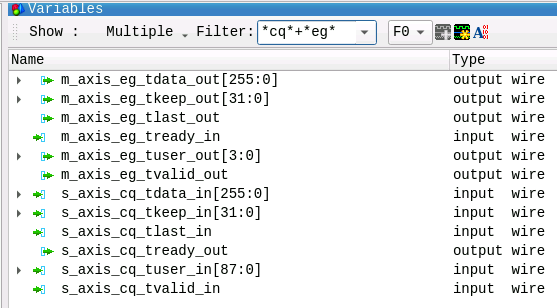
Figure 11 shows the Variables View with the filter set to input/output signal filtering and wildcards for the ntb_top module’s main TLP interfaces, CQ, which are ingress signals (*cq*) from RPA0 to UUT (connection C) and EG, which are egress signals (*_eg_*) at connection (D). The signals can easily be added to the waveform view by clicking on the waveform button in the top right corner.
To analyze the packets at the ntb_top interfaces CQ and EG Visualizer provides features to define Expressions/Functions on signals. To generate a signal valid_packets that shows TLP handshakes on the AXI interface, we insert an ‘AND’ expression which is set on TVALID, TLAST and TREADY for both interfaces. Figures 12 and 13 show how easy this is: Just select the signals with the cursor, right click and select ‘General Expression’.
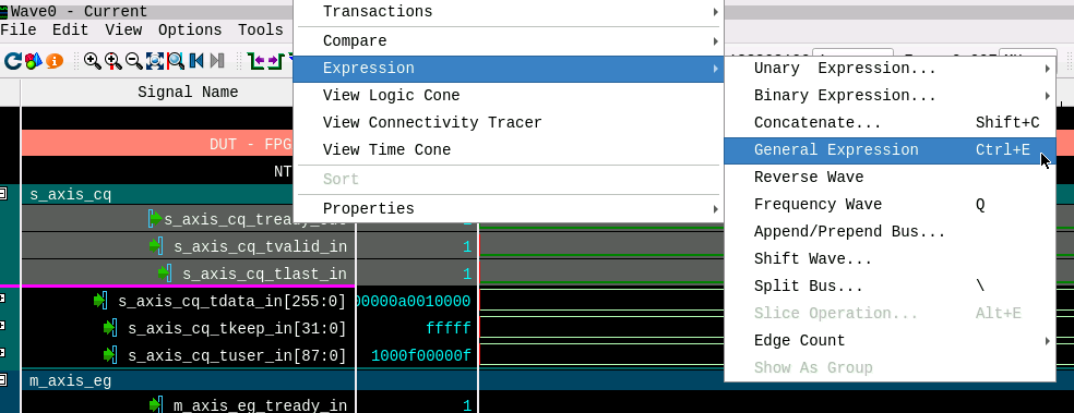
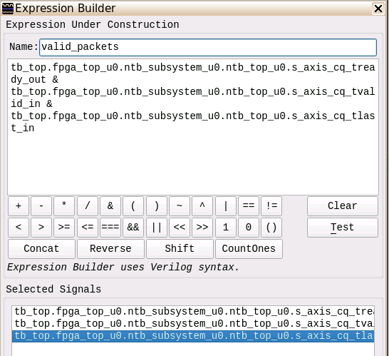
Figure 13 shows the Expression Builder View. We define an ‘AND’ expression on the selected signals for both interfaces. This newly created valid_packets signal we use to have Visualizer count the signal edges and in fact the number of TLPs. For debugging we wanted to know how many of the TLPs from interface (C) are being forwarded to interface (D). For this we use another builtin function of Visualizer: Counting Events shown in Figure 14 and Figure 15.
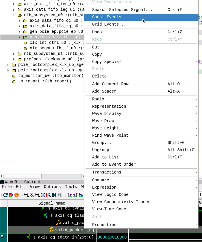
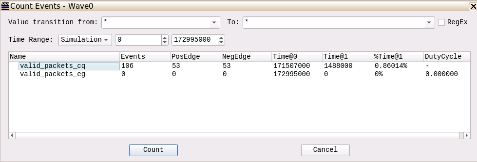
Figure 15 shows a total of 53 TLPs at the CQ interface, but 0 TLPs get forwarded by the NTB via EG interface. This indicates that TLPs get lost already inside the primary NTB module.
Visualizer provides another nice feature, Connectivity Tracer, shown in Figure 16 which we now use to trace the source of the EG interface packet assertion backwards.
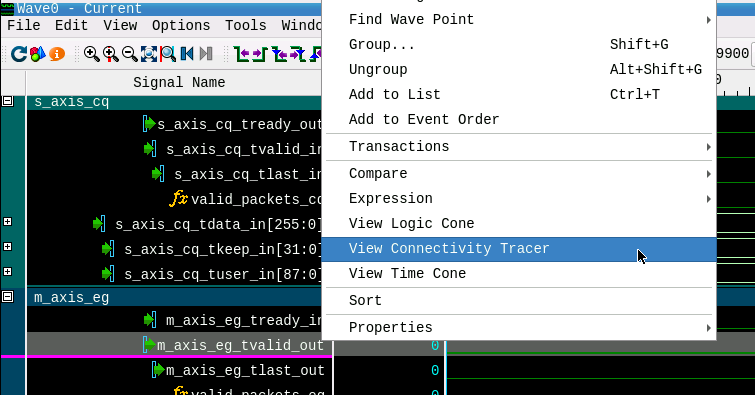
Simply right click in the EG’s TVALID signal and click on ‘View Connectivity Tracer’ to open the View.
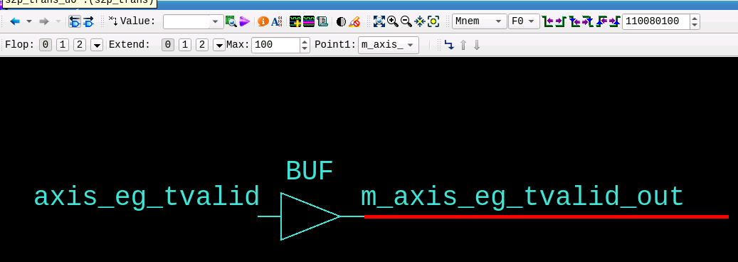
Double clicking on the left net expands the trace and shows the shows assignments highlighted in the source code view (see Figure 17). Expanding the trace leads us to the module p2s_trans that asserts the TVALID signal after parsing and translating the TLP.
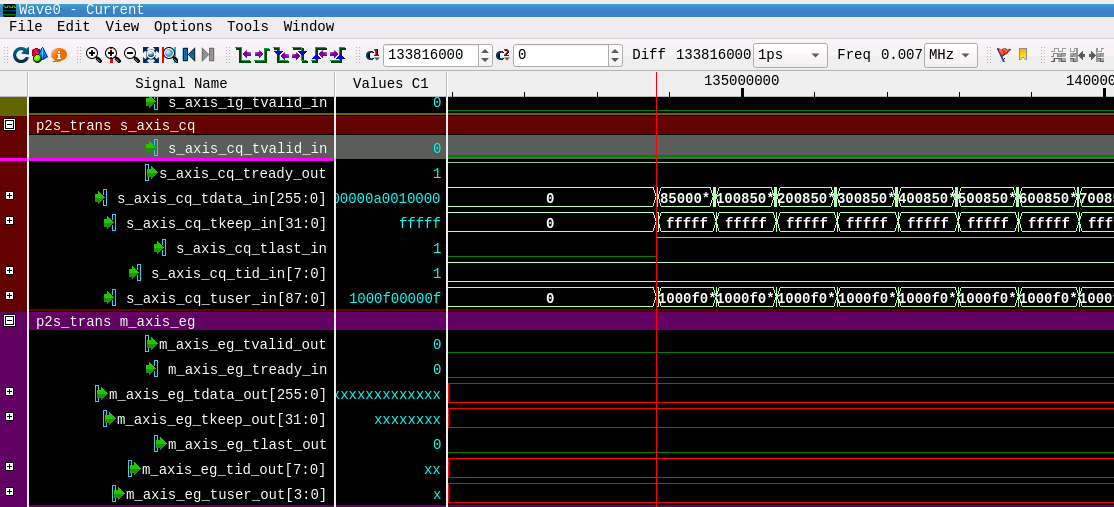
Figure 18 shows these interface groups CQ and EG of the module p2s_trans. The red lines in the waveform view of the AXIS EG interface group indicate that the AXI-Stream master interface does not forward any TLPs.
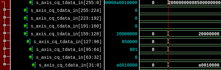
So, what exactly does the module p2s_trans do? The module processes the TLPs by slicing the header and retrieving the target address, performs the actual address translation and in case of an invalid access, drops the respective packet. To verify the module’s internal TLP Header decodings, Visualizer assists you with bus inspections. The TLP header may be sliced up into Doublewords (PCIe TLP Header format is in DWORD) using the ‘Expression’ → ‘Split Bus’ feature (see Figure 19).
As the module mainly parses the address field of the TLP to perform the translation, it may be convenient to check the address decoding by comparing the internally parsed values with the current address of TLPs. The data format for this PCIe Core transmits the 64-bit address in the first two DWORDS of a TLP. Using Visualizer’s GUI we combine the DWORDS into one signal by selecting the two immediate signals and right click → Expression → Concatenate.
For MLE NTB, the upper fields of the address encode the partition number to be accessed and the lower bits of the address are the actual address offset within a particular partition. Using Visualizer’s GUI, we slice the address field signal into both parts (63:25, 24:0) by right click → Expression → Slice Operation.
Next, we add the module’s internally decoded signals to the waveform view for comparison. Using Visualizer’s GUI we select both ‘address base offset’ signals and right click → compare → simple (see Figure 20).
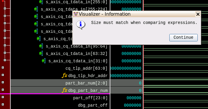
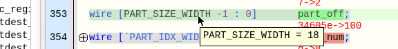
By comparing the partition number and address offset signals, the tool alerts that the signal vector widths do not match which points us to the actual bug. By double clicking on the signal in the waveform, the code view opens with the cursor set at the signal declaration. The signals’s width parameter may be seen (hexadecimal tooltip value) by mouse hovering over the parameter. The bug is now identified because the parameter shall be 24 instead of 25 (shown in Figure 21).
6. Conclusion
PCIe as the ubiquitous connectivity fabric between CPUs, GPUs and FPGAs adds additional challenges during debugging of distributed systems. The key point of this FPGA debugging example is that you do need a collection of tools and techniques in order to do your job efficiently: Xilinx XSim from the Vivado toolsuite can help you a lot. However, in case of debugging PCIe-based FPGA designs (eg, PCIe NTB), we recommend to add the fast RTL simulator Mentor Graphics Questa to your set of tools. Your debug turn-around-times will shorten significantly!
Complementing Mentor Graphics Visualizer further boosts the effectivity of Questa, first with a powerful GUI and second with its database that provides full design visibility.
Authors and Contact Information
Andreas Braun
Sr. Engineer
Missing Link Electronics GmbH
Endric Schubert
PhD, CTO
Missing Link Electronics, Inc.
Missing Link Electronics, Inc.
2880 Zanker Road, Suite 203
San Jose, CA 95134, USA
Missing Link Electronics GmbH
Industriestrasse 10
89231 Neu-Ulm
Germany
 www.missinglinkelectronics.com
MLE (Missing Link Electronics) is offering technologies and solutions for Domain-Specific Architectures, which focus on heterogeneous computing using FPGAs. MLE is headquartered in Silicon Valley with offices in Neu-Ulm and Berlin, Germany.