Integrated ADC for Altera Cyclone-IV Devices
This Technical Brief describes how to use Delta Sigma Modulation to implement resource-efficient Analog-to-Digital Converters (ADC) in Altera FPGA devices. Starting with an introduction into the technology of Delta Sigma Modulation, we will cover the relevant technical aspects for implementing and applying this as a flexible and cost-efficient means for ADC. We will provide the results of diligent testing using Altera Cyclone-IV FPGA devices which led to our technical specifications (Signal-to-Noise Ratios, Linearity, Spurious-Free Dynamic Range values).
Copyright © 2023 Missing Link Electronics. All rights reserved. Missing Link Electronics, the stylized Missing Link Electronics MLE logo are the service mark and/or trademark of Missing Link Electronics, Inc. All other product or service names and trademarks are the property of their respective owners.
Field-Programmable Gate-Arrays (FPGA) are well established for implementing programmable logic. A lesser known feature is their programmable digital I/O capabilities. Supporting Low-Voltage Differential Signaling (LVDS) at frequencies of many hundred MHz, FPGA pins have become a viable option for quality analog I/O. This Technical Brief shows how to implement Delta Sigma Analog-to-Digital Converters (ADC) inside Altera FPGA devices plus some additional passive components.
The result is a flexible integrated solution with smaller PCB footprint, field-upgradability and reduced risk of device obsolescence.
Key Features
- SNR 60 dB (compares to 10 bits effective resolution)
- Sample-rate up to 500 k samples per second
- Input range 0 to 3.3 V with high linearity, other input ranges are parameterizable.
- Cost-efficient for multi-channel-systems: 8 ADC channels use 801 LEs and 16400 memory cells.
- Resources < 121 LEs for Altera Cyclone-IV for the first instance. Futher instances use 68-72 LEs.
Areas of Applicability
- Flexible data acquisition systems
- Solution for “one more IO”-problems
- Integrated voltage monitoring system
- Instrumentation and control systems
- Sensor input in ambient intelligence
- Integrated microcontrollers with reduced risk of parts obsolescence
- Support of AM protocols like IRIG
The integrated ADC technology presented in this Technical Brief has undergone extensive testing and diligent analysis and has demonstrated to be robust and of high quality. When combined with the appropriate design methodology it is considered application-ready.
Concept
The basic theory behind the Delta Sigma Modulation is shown in Figure 1. The time-continuous signal x(t) is the input signal and the resulting output is the time-discrete digital y(z). A First-Order Delta Sigma Modulator comprises a feedback loop which subtracts the feedback signal from the input signal (delta). These differences are then summed up in the integrator (sigma).
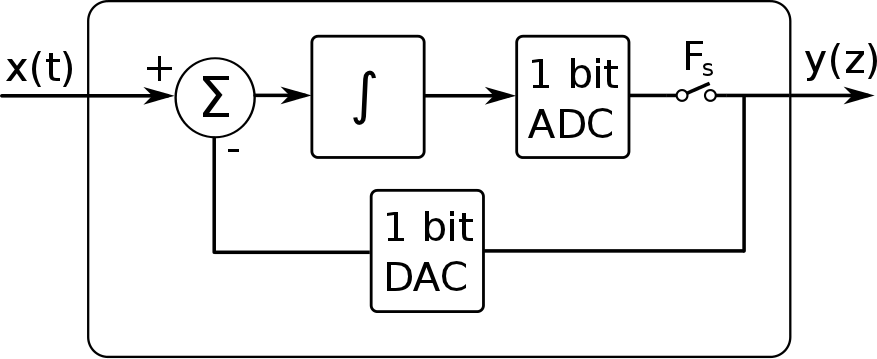
This feedback loop leads to the transfer functions of the First-Order Delta Sigma Modulator: H(z)signal = 1; H(z)noise = 1 -z-1 As these functions underline, the noise is high-pass filtered which is convenient looking at the other aspect of the Delta Sigma Modulation, the oversampling. With oversampling, we sample the analog input signal with a much higher frequency than the Shannon-Nyquist theorem demands. The result, in combination with the high-filtering effect of the Delta Sigma Modulator is, that the noise is distributed to the higher frequencies. This is called Noise Shaping. The possible signal-to-noise (SNR) ratio gain using oversampling is 3dB per octave. Using first order Delta Sigma Modulation, this SNR gain rises to 9dB per octave. These effects can be seen in Figure 2 a, b and c.
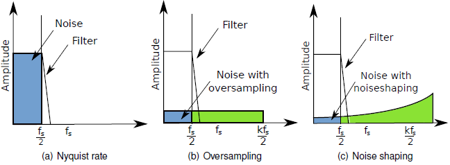
Figure 2 (a) shows the Nyquist Sampling converter. All quantizing noise is in the desired signal band. A first improvement comes from Oversampling and is shown ins Figure 2(b). It distributes the noise equally over the sample spectrum. A second improvement is Noise Shaping which is shown in Figure 2(c). Noise-shaping acts as a high pass for the noise and is the enabling piece which allows us to build high quality ADC inside purely digital FPGA devices.
However, the drawback of Noise Shaping is that one must come up with appropriate parameter sets to operate the inherently instable Delta Sigma Modulator.
Parameter Setting
To obtain suitable parameters for the Delta Sigma Modulator, a Matlab simulation was created. The design flow for the parameter creation can be seen in Figure 3:
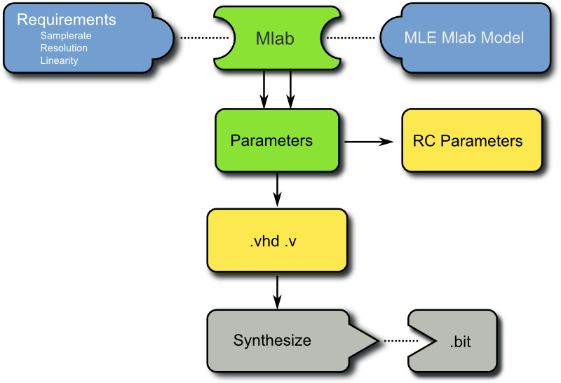
When running this parameter search, a parameter space is being searched to find the most suitable parameter set for the desired application. The parameter space addresses the integrator time-constant which is in this case a low-pass time-constant and the sample frequency which determines the oversampling frequency. An exemplary heat map of one of these simulations can be seen in Figure 4.
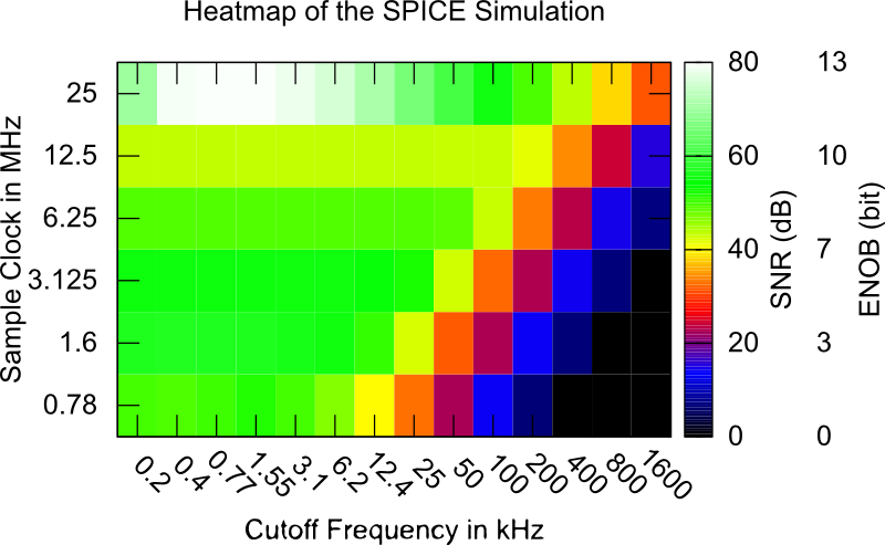
The heat-map is plotted by drawing the two different parameters over the resulting SNR value and shows two things. At first, it shows a good parameter set for the desired input frequency. It also shows that just using a higher sample frequency won’t automatically give better results unless you consider the other parameters such as the integrator time-constant.
So when actually parameterizing the hardware part of the Delta Sigma Modulator, on has to first decide for the desired ENOB or SNR. After that a suitable spot with enough reserve is chosen and results in a parameterisation of the Delta Sigma Modulator when the actual values for the resistors and the capacitor are calculated from the lowpass cutoff frequency.
Implementation
The basic components are shown in Figure 5. The external components are the two resistors and one capacitor. In combination with the Low Voltage Differential Signaling (LVDS) receiver and a Flip-Flop a Delta Sigma Modulator is built. Other components of the Delta Sigma Modulator ADC input are the Filters used to get the desired signal. There is the Moving Average Lowpass Filter with typically 1024 taps but can have whatever size required. The Decimation Filter samples the Data down to the desired sample-rate which is typically 48 KHz. After this there can optionally be a Calibration Filters for offset and gain compensation and Filters to remove AC components.
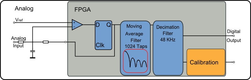
The Delta Sigma ADC was implemented using VHDL to support a wide range of target FPGA devices. It consists of several modules, namely the Delta Sigma Modulator which generates the bit-stream, a low-pass filter which cuts of the high band noise and prevents aliasing. The last module is a decimator filter which converts the signal to the desired sample rate and bit width.
Testing
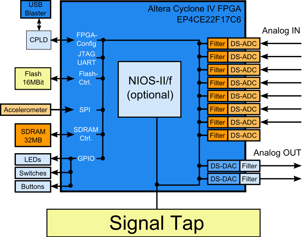
To validate the simulation results, diligent analysis was done. In particular we tested and measured the quality of results for Altera Cyclone-IV FPGA devices namely the EP4CE115, which is located on the Terasic Industrial Networking Kit (INK) DE2-115 board.
For example, values for the resistors and the capacitor were picked from simulation, and were determined to be 100 pF for the capacitor and 10 kOhm for the resistors which are values from the parameterization for a 100 Mhz bitstream sample rate.
During our tests we found out that the quality of the passive components has little effects on the overall quality of the ADC. For example, the resistors can be wired metalloxide resistors and the capacitor can be a styroflex capacitor. The voltage reference was created by a voltage divider from the 3.3 V Voltage source using two additional 10 kOhm resistors.
Crosstalk
Crosstalk is the influence of other ADC channels on the ADC. During our testing we found very little effects of crosstalk: For example, we implemented two Delta Sigma ADC on the same FPGA voltage bank. The measured channel had no input signal, and the other channel had a full scale 1 kHz input signal. The resulting signal on the channel with no input was measured and the resulting SNR was 2.3 dB.
Temperature Drift
For the influence of the temperature drift, we cooled the FPGA as well as the external circuitry down to a temperature of -40 ∘C and then back to room temperature. We could not detect any effects caused by temperature drift.
Linearity
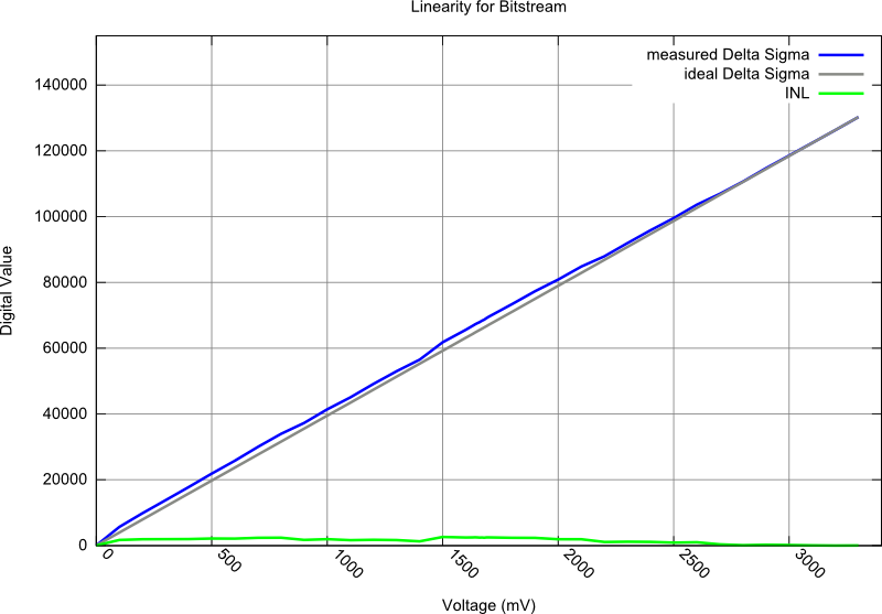
For linearity analysis an input signal was sampled and the resulting digitized bit stream was recorded using the Altera Signaltap integrated logic analyzer.
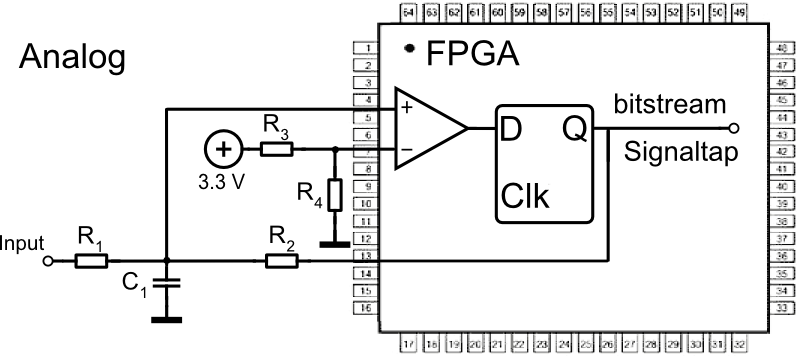
The measured sample depth was 65536 Samples. The clock speed of the Delta Sigma Modulator was 100 MHz. The example schematic can be seen in Figure 6. To analyze the linearity, voltages from 0 to 3.3 Volts were generated using an Agilent E3642A power supply. These voltages were verified using an Agilent 33410A high performance multimeter. The whole measurement was controlled by a Linux PC using the GPIB interfaces of the Voltage Source and the Multimeter. The results of the linearity measurement can be seen in Figure 7. The integrated nonlinearity (INL) plot demonstrates linearity over the entire voltage input range, as well as a strongly monotonic behavior. It also shows that the whole range from 0V to 3.3 V can be measured.
Quality of Results
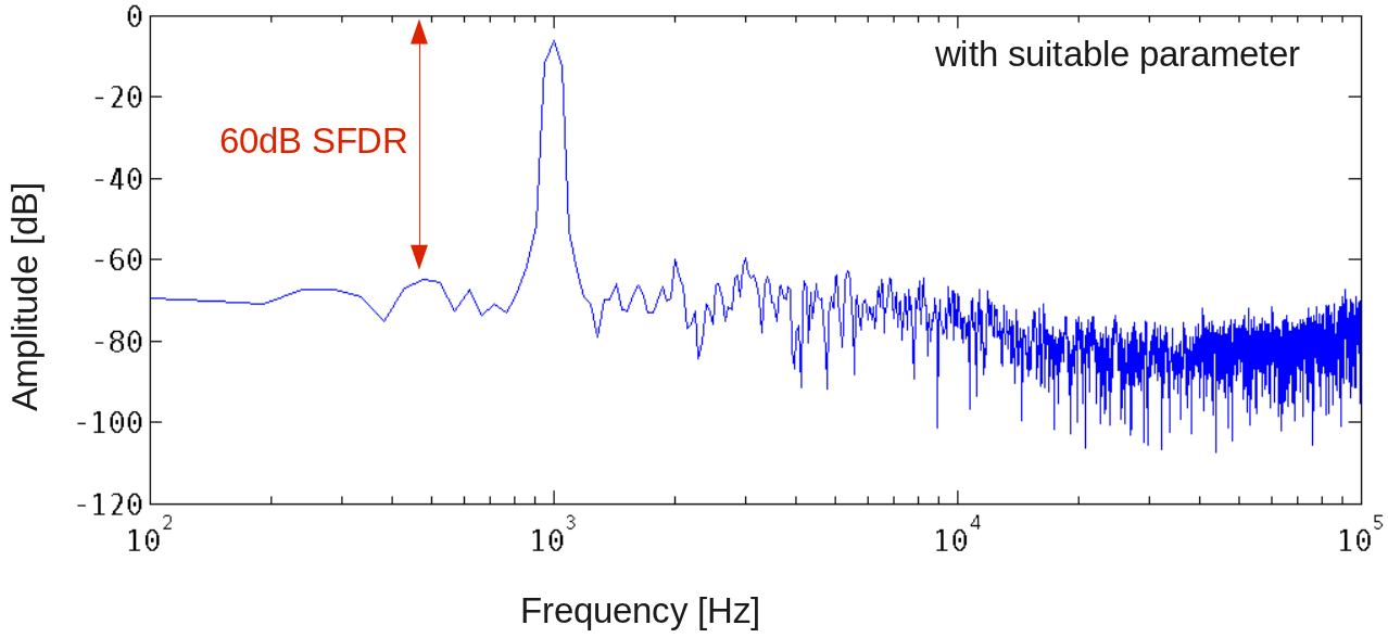
Other important parameters of an ADC are the Signal to Noise Ratio (SNR), the Spurious Free Dynamic Range (SFDR) and the Total Harmonic Distortion (THD). These values were measured using the same resistor / capacitor values (10 kOhm and 100 pF, resp.) as during the measurement of the linearity. These parameters have been measured using different input signal frequencies from 500Hz to 15 kHz and a sample frequency of 50 kHz with an oversampling ratio of 1024. The calculation of the SNR, the SFDR and the THD was done using Matlab.
| Frequency (Hz) | SNR (dB) | THD (%) | SFDR (dB) |
|---|---|---|---|
| 500 | 59 | 0.02 | 38 |
| 1000 | 56 | 0.025 | 39 |
| 5000 | 57 | 0.015 | 44 |
| 10000 | 54 | 0.01 | 47 |
| 15000 | 53 | 0.01 | 53 |
Figure 8 shows a Fourier spectrum with a good parameter set for the Delta Sigma Modulator. In this Fourier spectrum the 60dB SFDR can be easily seen.
Resource Requirements
The resource usage of the particular Altera Cyclone-IV design used in the analysis was 801 LEs plus two M9K elements for 8 separate ADC channels.
The main resources are needed by the filtering stage, the actual Delta Sigma Modulator just uses 1 LE. The standard input voltage range is from 0V to the full feedback pin voltage. It can be extended by using an op-amp to scale the input signal, or by changing the input resistor to a higher value.
Of course, when a higher input voltage is applied, measures should be taken to protect the FPGA input pin from over-voltage. One can achieve high quality of ADC results without high quality passive components for the Delta Sigma Modulator. This is an additional benefit of this method. The only requirements are that the integrator time-constant is matching the values calculated in the simulation.
Mixed Signal FPGA Development Kit for Altera Cyclone IV FPGAs
This kit allows easy and efficient evaluation of MLE’s soft ADC and DAC technology. The following components are included:
- Two boards, the Terasic DE0-Nano FPGA Development board featuring the Altera Cyclone-IV FPGA and the MLE passive-only Connector board.
- The MLE Evaluation FPGA reference design for the Altera Cyclone-IV FPGA.
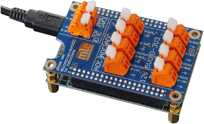
The Evaluation Git comes pre-assembled and pre-configured, ready to start evaluation.
Please visit
http://mlecorp.com/softadc
for the official Evaluation Guide or to apply for free evaluation.
Brief features summary:
- Altera Cyclone IV FPGA device
- 8 independent ADC channels, sampling at 48kSamples per second at 16 bits
- 2 ADC channels with 12V input
- 2 ADC channels with 5V input
- 4 ADC channels with 3.3V input
- 2 independent DAC channels
- 2 DAC channels with 3.3V output
- Pre-configured with 750Hz sine wave generators
- 1 DAC-to-ADC loop-back
- Optional: Altera NIOS II based System-on-Chip from MLE (not utilized in this evaluation)
Reference
[1] F. Sousa, V. Mauer, N. Duarte, R. P. Jasinski, and V. A. Pedroni, Taking advantage of LVDS input buffers to implement sigma-delta A/D converters in FPGAs. IEEE, 2004.
[2] M. Ortmanns, Personal Communication. 2010.
[3] E. Schubert, H. Zekel, C. Grumbein, and A. Zimmermann, FPGA can do analog! 2011.
[4] C. Grumbein, FPGA-Based first order Delta Sigma ADC. 2010.
🌐 www.missinglinkelectronics.com
MLE (Missing Link Electronics) is offering technologies and solutions for Domain-Specific Architectures, which focus on heterogeneous computing using FPGAs. MLE is headquartered in Silicon Valley with offices in Neu-Ulm and Berlin, Germany.