LVDS Connectivity for the MLE 1000 Series
This Technical Brief describes how to connect to certain modern cameras that provide a serialized protocol over a Low Voltage Differential Signaling (LVDS) interface. Utilizing the flexibility of today’s Field Programmable Gate-Array (FPGA) devices, the requirements for the I/Os are discussed first. Then an implementation is shown which implements a Data and Clock Recovery mechanism and a Synchronization and Packetization module in FPGA logic. The implementation has been tested and can serve serialized LVDS camera interfaces of 300 Mbps and higher.
While the approach has been implemented for and been tested on a Missing Link Electronics 1000 Series Rapid Prototyping System, it can easily be adapted to other FPGA-based electronic designs. It can also be extended to drive LVDS-based TFT displays.
Copyright © 2023 Missing Link Electronics. All rights reserved. Missing Link Electronics, the stylized Missing Link Electronics MLE logo are the service mark and/or trademark of Missing Link Electronics, Inc. All other product or service names and trademarks are the property of their respective owners.
One of our daily challenges here at Missing Link Electronics is to quickly and reliably connect various peripherals to a rapid prototyping system, to facilitate system-level testing of hardware and software together, for example. While this task is pretty straight forward in case of standard connectivity such as Ethernet, USB, Audio/Video, CAN, SPI, etc – our MLE 1000 Series Rapid Prototyping System has all this connectivity readily available – the real power of rapid prototyping lies in the ability to connect general purpose I/O via single-ended or low-voltage differential signaling (LVDS).
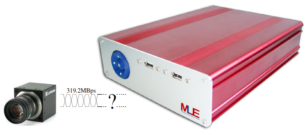
In one case we had to connect several video cameras to the MLE 1000 Series Rapid Prototyping System for video analysis to validate certain vision algorithms. Each camera was delivering an 8-bit grey-scale image with 752×480 pixels resolution at 60 frames-per-second; the pixel clock was 26.6 MHz. To make things tricky, a serializing protocol was used that delivered the image as a 319.2 Mbps data stream over an LVDS connection.
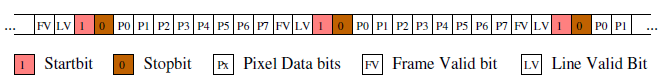
The good news was that we knew the serializing LVDS chipset inside the camera modules, so we knew the particular serial protocol: Each 8-bit pixel data (P0 to P7) was sent together with one data bit each for frame valid (FV) and line valid (LV). Embedded within this packet is the clock:
Instead, we decided to directly connect the cameras to our MLE 1000 Series Rapid Prototyping System and let the FPGA technology inside it do the electrical connectivity, the protocol and the data processing. In the past, we successfully had connected TFT displays directly to the MLE 1000 Series Rapid Prototyping System, so we knew that it could reliably handle high-speed LVDS connectivity.
This was made possible because of the flexible I/O technology inside modern FPGAs. Not only the high-end FPGA devices such as Xilinx Virtex-4, Virtex-5, Virtex-6, Altera Stratix IV, and Lattice ECP3 FPGAs have this powerful I/O technology, but also the low cost devices such as Xilinx Spartan-6 FPGA, or Altera Cyclone III, Cyclone IV FPGAs. You can find all this documented in the corresponding datasheets.
Our MLE 1000 Series Rapid Prototyping System uses the Xilinx Virtex-4 FX devices, for which the datasheet [UG70] lists in the I/O standards table 6-38 at page 299 all supported I/O configurations: the different voltage levels, different semantics of TTL and – very important in this case – LVDS.
So first, the Virtex-4 devices directly support LVDS standard at the I/O pins which was required by the camera modules. Second, the MLE 1000 Series Rapid Prototyping System provides an extension header which is connected to a separate I/O bank of the FPGA using length-matched 50 Ohms wire-pairs for LVDS (sometimes, on other boards all I/O banks of the FPGA routed to the extension headers are tied to the “wrong” standard with no possibility for change). Third, the MLE 1000 Series Rapid Prototyping System has a programmable clock chip which provides multiple clock signals which can be adjusted appropriately to match the required clock speed — in our case 320 MHz (which in combination with our de-serializer logic described below was close enough to the required frequency of 319.2 MHz). A programmable clock chip is not that important if you use FPGA devices which have built-in PLLs, such as Xilinx Virtex-5, Virtex-6, or the Altera Stratix IV devices.
Therefore, the problem of electrical connectivity – available, LVDS-capable extension headers with the correct voltage level and clock speed – was solved, and the next step was to implement a de-serializer protocol to extract the pixel data from the bit stream.
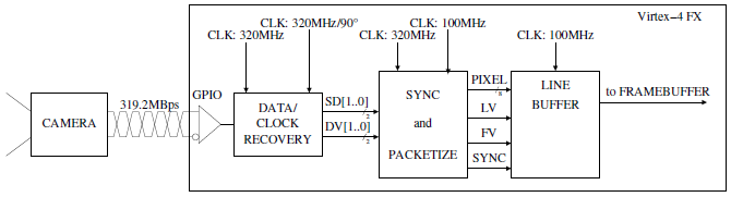
The block diagram (Figure 3) of our solution shows the serialized 319.2 Mbps bit stream entering the FPGA to be processed by a Data and Clock Recovery module. The output of the Data and Clock Recovery is the payload bits extracted from the bit stream. These bits can be one of the eight pixel data bits P0 to P7, the frame valid (FV) bit, the line valid (LV) bit, or the start or the stop bit.
The Sync and Packetize module implements the appropriate de-serializing protocol which synchronizes with the bitstream and extracts the 8-bit pixel data, the LV bit and the FV bit from the bit stream. These data bits are then used by a linebuffer to re-assemble the lines of the camera images which then go into a frame buffer.
The foundation of the Data and Clock Recovery module is described in Xilinx application note [XAPP224]: Using a first clock signal of 320 MHz and a second clock signal of 320 MHz shifted in phase by 90 degrees with respect to the first clock, the 319.2 Mbps bit stream is sampled 4 times. The logic inside the Data and Clock Recovery module selects the best sample by looking for edges in the transmission. As a result, during each 320 MHz clock period one out of three cases can happen: No sample bit was selected, one sample bit was selected or two sample bits were selected from the bit stream at the same time. The zero, one or two sample bits are stored in the sample data SD[1..0] and it is marked that the particular sample data bit is valid by putting a ’1’ into the corresponding data valid DV[1..0]. By 4-times sampling the Data and Clock Recovery module becomes robust against clock jitter and relaxes the need to have the clock signal exactly match the LVDS frequency.
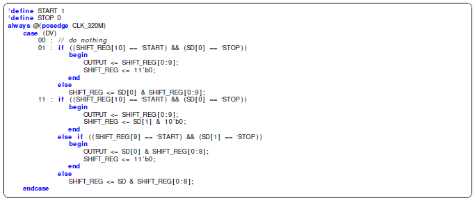
The Sync and Packetize module has a 320 MHz clock signal to read the SD[1..0] and DV[1..0]. In a first step, at 320 MHz it detects the start bit (always one) – stop bit (always zero) combination from the serial bit stream. This is not trivial, because during each clock period zero, one or two data bits can enter the Sync and Packetize module and each case has to be dealt with differently. The solution to this de-serializer protocol is shown in the Verilog HDL code section below.
‘define START 1
‘define STOP 0
always @(posedge CLK_320M)
    case (DV)
        00 : // do nothing
        01 : if ((SHIFT_REG[10] == ‘START) && (SD[0] == ‘STOP))
                begin
                    OUTPUT <= SHIFT_REG[0:9];
                    SHIFT_REG <= 11’b0;
                end
             else
                SHIFT_REG <= SD[0] & SHIFT_REG[0:9];
        11 : if ((SHIFT_REG[10] == ‘START) && (SD[0] == ‘STOP))
                begin
                    OUTPUT <= SHIFT_REG[0:9];
                    SHIFT_REG <= SD[1] & 10’b0;
                end
             else if ((SHIFT_REG[9] == ‘START) && (SD[1] == ‘STOP))
                begin
                    OUTPUT <= SD[0] & SHIFT_REG[0:8];
                    SHIFT_REG <= 11’b0;
                end
             else
                SHIFT_REG <= SD & SHIFT_REG[0:8];
    endcase
The serial to parallel conversion uses an 11-bit shift register (SHIFT_REG[0..10]) into which the one or two entering data bits are stored. If the first position (SHIFT_REG[10] or SHIFT_REG[9], depending on the case) matches the start bit (always one) and the last position (SD[0] or SD[1]), depending on the case) matches the stop bit (always zero), then we have may assembled a correct and complete packet of 8-bit pixel data plus frame valid and line valid bits.
To avoid false positives, the de-serializer protocol must have successfully assembled a larger number of correct and complete packets in a row, before it considers itself “in synchronization” with the serial bit stream and before the packets can actually be delivered. In our implementation we use a counter to check whether 128 packets have been assembled in a row. Once “in sync”, a loss of synchronization can be detected by an overflow of the shift register, which is done by counting the number of bits in the shift register; in this case the Sync and Packetize module must restart. For verification purposes, especially if you implement your own de-serializer protocol, we strongly recommend using a built-in logic analyzer (Xilinx ChipScope, Altera SignalTap, Synopsys Identify) which triggers on loss of the synchronization. In our testing we could not detect any loss of synchronization during six hours of continuous operation.
To relax the timing constraints on the design we used a handshake protocol to switch over from the 320 MHz clock domain to a less demanding 100 MHz clock domain in which the further processing happens. Therefore, the Sync and Packetize module also has a 100 MHz clock signal input which is used for handing over the 8-bit pixel data, the frame valid and the line valid bits to the Linebuffer module. Because the pixel data rate is 26.6 MHz, a packet of 8-bit pixel data, frame valid and line valid bits are handed over approximately every fourth period. By analyzing the frame valid bit and the line valid bit the Linebuffer module assembles a whole line of pixels which are then transferred using a PLB IPIF [DS448] based busmaster core to main memory, where the lines are directly assembled to a frame in the framebuffer.
For efficiency and data integrity reasons – the transfer latency to RAM via the Processor Local Bus (PLB) is unknown – we implemented a double buffer technique using a BRAM module. Extra attention is required when setting the IP2IP_Addr in the PLB IPIF. This can either result in a non working IP-Core (if IP2IP_Addr is not within the memory range of the core) or in data corruption (if a 32 bit alligned address (IP2IP_Addr[29] == ’1’) is used for 64 bit transfers). Both errors are hard to catch during runtime.
In our Xilinx Virtex-4 FX FPGAS based MLE 1000 Series Rapid Prototyping System, the implementation of the Data and Clock Recovery module plus the Sync and Packetize module needed less than 100 slices per camera. Our timing analysis had shown that for a device speed grade of -12 our solution can operate up to 400 MHz and thus can serve even faster LVDS-camera interfaces reliably. As a result we are proud to show a single-camera setup of the MLE 1000 Series Rapid Prototyping System to film the hardware platform of another MLE 1000 Series Rapid Prototyping System.
References
[UG70] Xilinx, Inc.:
Virtex-4 FPGA User Guide, December 2008.
http://www.xilinx.com/bvdocs/userguides/ug070.pdf
[XAPP224] Nick Sawyer, Xilinx, Inc.:
Application Note 224: Data Recovery, July 2005.
http://www.xilinx.com/support/documentation/application_notes/xapp224.pdf
[DS448] Xilinx, Inc.:
PLB IPIF(v2.02a): Product Specification, April 2005.
http://www.xilinx.com/support/documentation/ip_documentation/plb_ipif.pdf
🌐 www.missinglinkelectronics.com
MLE (Missing Link Electronics) is offering technologies and solutions for Domain-Specific Architectures, which focus on heterogeneous computing using FPGAs. MLE is headquartered in Silicon Valley with offices in Neu-Ulm and Berlin, Germany.