Configurable Systems in Altera Stratix-IV FPGAs
This Technical Brief describes a Configurable System based on Altera’s Nios-II processor running MLE’s “Soft” Hardware Platform, integrated into Terasic’s DE4 Development Kit. The system implements a complete Single-Board Computer (SBC) which supports a multistage boot process to provide software-based flexibility for different Linux software stacks.
Copyright © 2023 Missing Link Electronics. All rights reserved. Missing Link Electronics, the stylized Missing Link Electronics MLE logo are the service mark and/or trademark of Missing Link Electronics, Inc. All other product or service names and trademarks are the property of their respective owners.
Missing Link Electronics (MLE) has developed a validated methodology for hardware / software co-design and systems realization. Based on this, MLE provides configurable processing solutions based on off-the-shelf components running a full Open Source software stack. This is integrated into a pre-validated systems development and prototyping platform where hardware and software can be customized for the target application.
Field-Programmable Gate-Arrays (FPGAs) are the foundation semiconductor technology behind these Configurable Systems – they offer additional degrees of freedom for cost and performance optimizations, the flexibility to perform changes throughout the embedded products life-cycle and can protect from device obsolescence.
Altera’s Nios-II is a 32-bit RISC microprocessor1 available as a so-called soft IP core for implementation inside Altera FPGA devices. Combine the Nios-II CPU with a memory management unit (MMU) and custom I/O connectivity and you have a key building block for implementing Configurable Systems.
The DE4 Development Board from Terasic Technologies Inc. is a versatile FPGA development hardware for embedded systems. The DE4 includes an Altera Stratix IV GX230 FPGA with an option to upgrade to a Stratix IV GX530. The capacity of either FPGA device is huge and allows to implement powerful systems-on-a-chip with custom processing for signal analysis, for example.
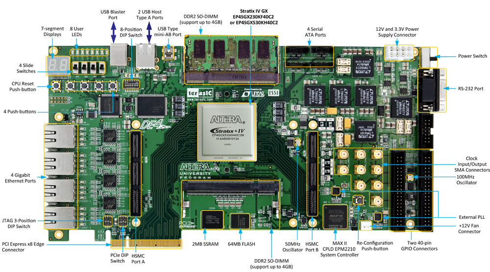
The DE42, as shown in Figure 1 comes with a variety of different connectors and interfaces to build a complete system. These include high-speed serial I/O for Serial ATA, for example, two DIMM connectors for DDR2 memory, USB 2.0, etc. For details we recommend the user manual of the Terasic DE4 Development Board3.
MLE considers the Terasic DE4 to be a flexible and well engineered hardware board for the development and prototyping of custom embedded systems. Therefore, MLE provides a pre-validated “Soft” Hardware Platform for the DE4 which effectively turns the DE4 into a complete Single-Board Computer (SBC) running GNU/Linux. As such the system features:
- Application SW – GNU/Linux root filesystem with 500+ packages
- Operating System – U-Boot loader plus multiple variants based on Linux kernel 3.0
- System-on-Chip – 32-bit Nios-II/f at 175 MHz and 256 MB DDR2 RAM, SPI, Ethernet
- FPGA Device – Altera EP4SGX230 or EP4SGX530
- PCB and Connectivity – 64 MB on-board NOR flash memory, SD card, USB 2.0, SATA 6 Gbps, Gigabit Ethernet, RS232, GPIO
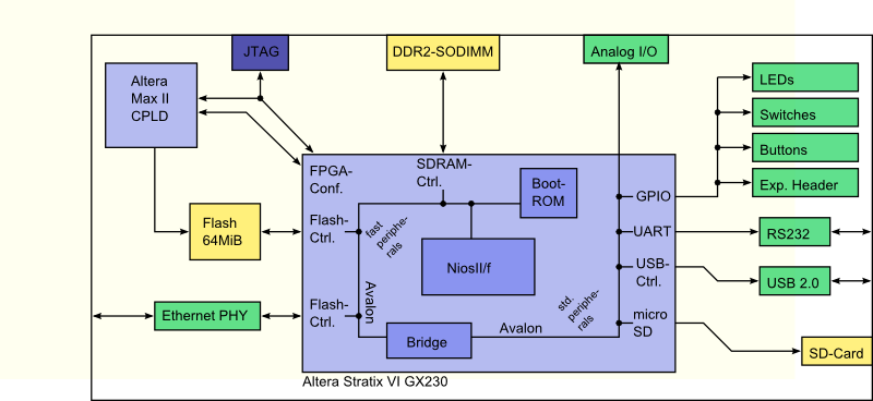
We preconfigured the Altera Stratix IV with a System-on-Chip based on the Altera Nios-II/f microprocessor including a MMU. This way the system can run a modern operating system (OS), GNU/Linux. The System-On-Chip connects to one of the two on-board DDR2-SoDIMM slots and is configured to use 256 MB as main memory, 64 MB on-board parallel flash, a SD-Card in SPI mode, one of the four Gigabit Ethernet as Eth0 device, a USB 2.0 complient High Speed only host, one EIA232 standard UART and several GPIOs. The blockdiagramm in Figure 2 shows how these peripherals are connected to the main CPU using the Altera Avalon bus.
As with all MLE supported platforms, MLE provides a full software stack, tightly integrated with the System-On-Chip. This software stack comprises multi-stage bootloaders, and a Linux operating system kernel. Supporting GNU/Linux as an operating system guarantees long term availability and delivers a high quality state-of-the-art implementation of a many protocols, drivers and userspace programs.
Of course there is more to a system than a kernel, so MLE also provides a rich environment of pre-compiled and pre-installed GNU/Linux software packages, delivered on a root filesystem. Obviously all the software packages can be re-built via the MLE distribution builder tool. While the same tool is used for all supported platforms, not all components may be interchangeable between these platforms. These limitations come from the tight integration of software and hardware and MLE’s support for multiple other processor architectures such as ARM or PowerPC.
The Altera Nios-II CPU is an ideal CPU for Configurable Systems because it can be augmented via custom instructions and hardware co-processing, for software acceleration. However, from a compute performance it targets the deeply embedded applications which run with very limited graphics requirements. That is why MLE Linux for the DE4 (and other supported platforms like the MLE “Soft” Hardware Platform for the Altera BeMicro SDK) is a console-based Linux. Yet, it comes with a state-of-the-art Linux kernel 3.0 and, of course, a powerful embedded boot process with the flexibility of multiple init states. As part of the Linux ecosystem a lot of functionality comes on the side:
- multi-user, multi-tasking operation,
- scheduling tasks via cron,
- disk storage management via mount, fdisk, fsck
- network deamons like webservers, telnet, ssh or even network based storage via nfs,
- remote-procedure calls similar to SOAP,
- secure file transfers with strong encryption, e. g. via scp,
- lightweight package-based software lifecycle management, e. g. via opkg.
Like any embedded Linux system, it comes with a flexible system boot process, as shown in Figure 3 which is fundamentally different from an ASIC microcontroller or PC-based boot process: The underlying FPGAs are SRAM based, i. e. they must be configured with a bitstream to implement a digital circuit design when the power comes up. So the first thing on the DE4 board to do at power-on is to configure the FPGA with an MLE-provided bitstream, effectively implementing the System-on-a-Chip. This configuration step is done by the Altera Max-II CPLD which readd from the on-board flash memory and uploads the configuration bitstream into the FPGA via a passive parallel configuration port.
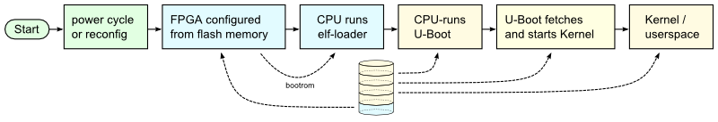
Once the CPLD has configured the FPGA, the boot process is very similar to other embedded systems. The Nios-II in the MLE Linux System-on-Chip design starts executing its initial boot program. We have configured the Nios-II in our “soft” Hardware Platform to load a small initial program from on-chip ressources. All this initial program does is to fetch a customized U-Boot loader from the on-board flash memory and to transfer control to this instance of U-Boot.
The U-Boot is a very flexible and, yet, dependable piece of Open Source software4 and well established in the embedded world. Most of the boot flexibility of the DE4 platform is achieved by using this bootloader. By default, we have configured U-Boot to determine the operating system kernel, which will be booted, user-controlled via DIP-Switches on the DE4 board. Additionally, a user-driven interactive mode – via a serial connection between the DE4 embedded target and a host workstation – is also possible. Multiple operating system kernels can be placed at different storage locations. During development typical places for U-Boot to load the kernel from are a network location (via TFTP, for example) or the on-board connected SD-Card. For a production system the operating system kernel most likely will reside in the on-board flash memory.
U-Boot not only loads the kernel into memory, but can also load a description of the System-on-Chip, the so called device tree, to the right position in memory. The device tree is standardized under IEEE 1275 Open Firmware and describes the underlying hardware (i. e. processing system with peripherals) from the software’s point-of-view. This way when U-Boot transfers control to the Linux kernel, the kernel can analyze the device tree description to obtain full information about the system. For an FPGA based system such a boot process has the great benefit of being able to change the System-On-Chip without the need to recompile the kernel. The Linux kernel itself, after initiating the known devices, finally mounts a root filesystem from either USB-Stick, SD-Card or via Network File System (NFS).
By default, MLE’s support for the Terasic DE4 comes with three variants of Linux: 1) A rescue system (known from the MLE 1000 Series Rapid Prototyping System) supports basic means of restoring a system image and checking the functionality of the hardware. 2) A development variant with network based booting from a TFTP server which allows very short turn-around-times during operating system and device driver development. And 3), a production variant that provides a pre-validated system software stack for a complete Single-Board Computer, built on top of the DE4 hardware.
Unfortunately, the current DE4 hardware lacks certain functionality for implementing hardware watchdogs and for handling multiple FPGA configuration bitstream. One work-around requires to rewrite a memory region in the on-board flash and to subsequently issue a reconfiguration of the FPGA device via software. For the benefits of watchdog mechanisms in Configurable System development please refer to our Technical Brief “Advanced Programmable System Configuration Management”5.
We have shown within this Technical Brief, how to take advantage of a multistage boot process to provide software-based flexibility to the Terasic DE4. We have also shown that multiple software variants for the DE4 are very feasible, making development easier for many target applications. This results in the Terasic DE4 becoming a full Single-Board Computer for the development and for prototyping connected embedded systems.
Reference
- ALTERA CORPORATION. Nios II – The World’s Most Versatile Embedded Processor.
http://www.altera.com/devices/processor/nios2/ni2-index.html ↩︎ - TERASIC TECHNOLOGY, INC. layout_1000.jpg
http://www.terasic.com.tw/attachment/archive/501/image ↩︎ - TERASIC TECHNOLOGY, INC. DE4 User Manual, August 2010.
http://www.terasic.com ↩︎ - DENX SOFTWARE ENGINEERING. Das U-Boot – the Universal Boot Loader
http://www.denx.de/wiki/U-Boot ↩︎ - MLE TECHNICAL BRIEF 20100817. Advanced Programmable System Configuration Management, 2010. ↩︎
🌐 www.missinglinkelectronics.com
MLE (Missing Link Electronics) is offering technologies and solutions for Domain-Specific Architectures, which focus on heterogeneous computing using FPGAs. MLE is headquartered in Silicon Valley with offices in Neu-Ulm and Berlin, Germany.