Please fill in the form below, so we can support you in your request.


    ASICAMD (Xilinx)AchronixIntel (Altera)LatticeMicrochip (MicroSemi)Other

    By submitting this form you are consenting to being contacted by the MLE via email and receiving marketing information.

    X
    CONTACT MLE
    CONTACT MLE
    We are glad that you preferred to contact us. Please fill our short form and one of our friendly team members will contact you back.


      ASICAMD (Xilinx)AchronixIntel (Altera)LatticeMicrochip (MicroSemi)Other

      By submitting this form you are consenting to being contacted by the MLE via email and receiving marketing information.

      X
      CONTACT MLE

      Facilitating Work-From-Home For FPGA Designers

      Facilitating Work-From-Home For FPGA Designers

      The Coronavirus forces us FPGA designers to work from home (WFH) while still facing challenging engineering deadlines…

      So, how can we work from home efficiently doing FPGA design, which typically requires access to FPGA hardware? Taking those FPGA boards home may not be the best option – particularly not when we need to collaborate through shared hardware / Devices-under-Test (DUT).
      MLE, a Premier AMD/Xilinx Alliance Partner, has faced similar challenges and has put together a solution for remote and shared access to FPGA boards.

      MLE, a Premier AMD/Xilinx Alliance Partner, has faced similar challenges and has put together a solution for remote and shared access to FPGA boards.

      Shared Remote Access to FPGA Hardware

      Application Use Cases

      • Enable secure remote access from home to shared FPGA hardware in corporate labs
      • Interactive development & debugging
      • Automated testing and Continuous Integration for FPGA-based system

      Key Benefits

      • Compatible w/ corporate VPN setups
      • Centralized DUT administration
      • Transparent “who is currently using the shared FPGA hardware?”
      • Efficient remote debugging with remote power cycling, when needed
      • Remote FPGA config and boot-up
      • Integrated w/ AMD/Xilinx Vivado Hardware JTAG Servers
      • Interact with serial console (AMD/Xilinx FSBL, U-Boot, Linux)
      • Interfaces with GPIO, UART, JTAG, USB-SD-Muxes and wireless SD cards
      • Independent from DUT software stack
      • User customizable and maintainable

      Availability

      • Builds on top of Open Source Labgrid
      • Licensed under open source LGPL
      • Per site NRE install fee $4,800.-
      • Extra integration & support services available at $980.- per engineering day
      LabGrid

      Setup for Shared Remote Access to FPGA Hardware

      Building upon Labgrid – an embedded board control Python library with a focus on testing, development and general automation – MLE provides setups for shared remote access to FPGA hardware.

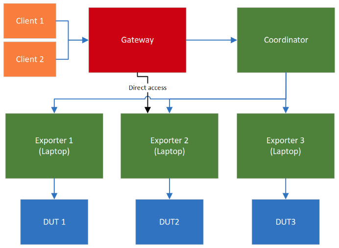
      The client (developer at home) connects to the gateway. The gateway can be a VPN server or a dedicated PC connected to the lab LAN.

      The client can acquire a lab setup of a DUT (forming a “place”) via the coordinator. Then defined interfaces and functions are directly exported to the client, like

      • power distribution unit
      • JTAG
      • UART – console interaction
      • Wireless SD cards and USB-SD-Mux – allows to change the SD card content
      • GPIO
      • USB WebCam – remote lab setup observation
        If more direct access is needed, the client may directly connect to the exporter host.

      If more direct access is needed, the client may directly connect to the exporter host.

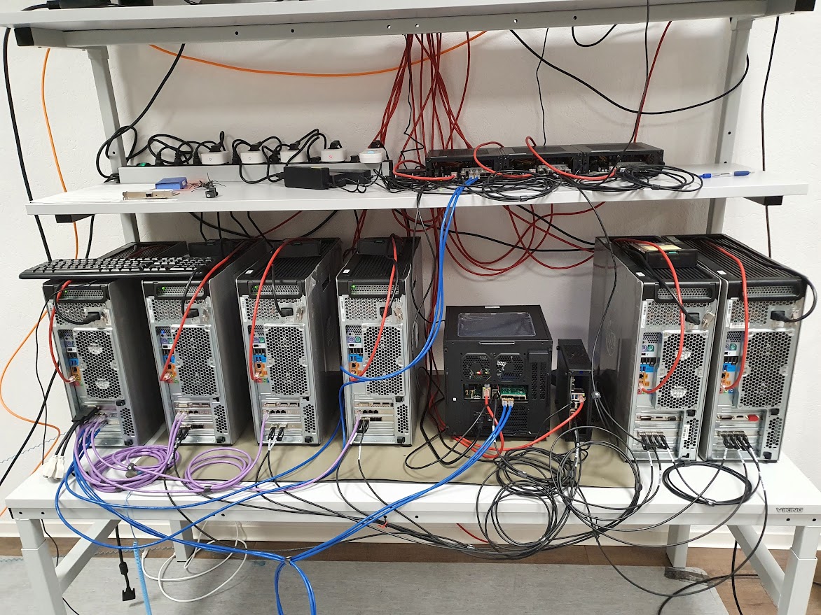
      Example for Shared Remote Access to FPGA Hardware

      Shared Remote Access to FPGA Hardware Example

      An example workflow, that acquires the place, turns on power and accesses the serial console
      looks like this:

      labgrid-client -p place-1 acquire
      labgrid-client -p place-1 power on
      labgrid-client -p place-1 console
      (do work on console)
      labgrid-client -p place-1 power off
      labgrid-client -p place-1 release

      Labgrid ensures that a place cannot concurrently be acquired by multiple clients. This eases up
      coordination when developers are not working physically close to each other in the lab.

      Design Methodology

      FPGA Design Methodology

      Design Methodology

      FPGA Design Methogology

      Alan Kay once said: 

      “People who are really serious about software should make their own hardware!”

      Many decades later, Dennard’s scaling (the increase of clock frequency with each node size shrink) has stopped. In result, next year’s CPUs just don’t get much faster anymore. Hence, large companies like Apple and Google, for example, employ in-house teams of chip designers for implementing custom System-on-Chips and ASICs to optimize software-rich systems via so-called Domain-Specific Architectures.

      Other companies have been relying on us, Missing Link Electronics, to achieve the same effects for software performance and/or battery life optimization. To reduce NRE costs and risks instead of custom ASIC we integrate programmable logic and SoC FPGAs from vendors AMD/Xilinx, Intel PSG, Microchip, Lattice and else. Here some key aspects of our design methodology which enables us to deliver predictable success:

      Systems Realization requires sophisticated hardware / software partitioning to meet the cost, performance and functionality targets. In general, embedded system designers have to find a solution within the multi-dimensional space of

      • Behavior – the correct functioning for each use case.
      • Timing – performance as well as real-time aspects.
      • Concurrency – parallel handling of user and environmental requests.
      • Structure – for example, for manufacturing, servicability, reliability reasons.

      MLE has specialized in design methodologies for finding appropriate solutions on time and on budget. These design methodologies comprise:

      • Rapid Prototyping and Virtual Prototypes
      • Platform-Based Design
      • Hardware / Software Co-Design and Co-Verification

      Systems Realization

      Systems are more that the sum of their parts! And especially Embedded Systems are more than just hardware and software!

      To build better Embedded Systems, faster, MLE utilizes state-of-the-art techniques for Systems Realization:

      • Transaction-Level Modeling – which is a powerful concept for architectural exploration and analysis at Electronic-System-Level (ESL). Based on the IEEE 1666 SystemC language standard subsystems implemented in VHDL or Verilog Hardware Description Language (HDL) – a.k.a. the Hardware – can be brought together with subsystems implemented in C or C++ – a.k.a. the Software.
      • Virtual Platforms (VP) such as QEMU from the Open Source ecosystem or the Virtual System Platform from Cadence Design Systems, Inc. which generate executable system models very early-on during the development phase when target hardware may not even be available.

      Because these techniques offer important design visibility for the optimization, verification and debugging of complex Embedded Systems MLE will continue adopting new techniques for Systems Realization.

      Hardware-Software Co-Design

      MLE applies modern concepts of Hardware / Software Co-Design to the design of cost, performance, and power-driven Embedded Systems. The results are micro-architectures which are highly optimized towards the target application and, yet, are within a development project’s time and budget.

      The classical bottum-up approach leaves design projects with an incomplete system lacking full functionality until the very last component has been implemented, integrated and tested. MLE proposes a top-down design methodology where all vital functionality is provided by proven Open Source software from the very beginning. Subsequent iterations of cost, performance and power analysis with state-of-the-art tools then drive the migration of functionality between software and hardware for acceleration.

      MLE’s Hardware / Software Co-Design methodology supports so-called companion chip solution where an FPGA device is loosely-coupled to a CPU via PCI Express, for example. It also applies well to modern devices such as Xilinx’ Extensible Processing Platform which support tight-coupling between the CPU and the programmable logic. By combining sequential processing in standard CPUs with fast, parallel execution in programmable logic the system’s bandwidth and latency can significantly be improved, as it is described, for example, in the article “Building a Better Crypto Engine the Programmable Way” in Xcell Journal.

      Platform-Based Design

      Described by Professor Alberto Sangiovanni-Vincentelli from the University of California, Berkeley, as “Freedom from Choice!” Platform-Based Design and Component-Based Design are powerful methodologies. MLE applies these techniques to Embedded System design because of their great potentials. The combination of off-the-shelf components with a rich Open Source software stack delivers processing platforms which are:

      • Complete enough – to significantly reduce design complexity and, thereby, development costs and risks
      • Versatile – to be customizable, at hardware and at software level, for many target applications
      • Powerful – by combining standard processing with application specific co-processing
      • Cost efficient – from a development and from a bill-of-materials perspective to become viable solutions for industrial and automotive applications.

      MLE’s “Soft” Hardware Platform makes it easy to take advantage of new programmable device technology such as Extensible Processing Platforms.

      Accelerating Machine Learning

      Accelerating Machine Learning

      Accelerating Machine Learning

      Accelerating Machine Learning

      Machine Learning in form of Deep Convolutional Neural Networks has demonstrated significant advantages over classical algorithms, however at the cost of a significant compute burdon. MLE has started putting together a set of accelerated platforms, solutions and focused services within the Xilinx FPGA ecosystem.

      Currently, these accelerated platforms, solutions and services focus on the Inference phase of Deep-Learning. MLE’s acceleration techniques for Deep Convolutional Neural Network Inference combine “unconventional” dataflow-oriented architectures with modern design flows using Xilinx High-Level Synthesis, and the Xilinx SDx tool chain.

      Close collaboration with re-knowned experts from the Bavarian Multi-Media Lab at Augsburg University, Germany, facilitates rapid adoption of recent research results, for example, in the field of Reduced Precision Neural Networks.

      MLE is a licensee of Xilinx and offers sub-licensing, technology support and complementary design services for integrating Accelerated Deep-Learning Inference into your application. When applied to the Deep-Learning Inference phase, Xilinx FPGA technology can provide a unique combination of low-latency response times, high compute performance in the Tera-OPS range, at very low Wattage.

      Applications of Machine Learning

      • Image processing and classification
      • Environment perception
      • Multi-camera object recognition systems
      • Sensor fusion

      Core Benefits

      • Very fast response time with low deterministic processing latencies
      • Very high, raw compute performance up to tens of Tera OPS
      • Low power envelopes of typically less than 50 Watts
      • Scalability from embedded system, to High-Performance Compute (HPC)

      Key Features

      • Highly integrated single-chip solutions
      • Scales to state-of-the art networks (CNV, ResNet-50, etc)

      Documentation

      AMD / Xilinx FPGA Design Services

      AMD/Xilinx FPGA Programming and Design Services

      Today, FPGA programming and design is far more than implementing glue logic. With the complexity of today’s FPGA devices it becomes cost-efficient to implement programmable system-on-chip solutions with multiple processor cores, heterogeneous accelerators and peripheral blocks interfacing with multi-gigabit transceivers, for example. Therefore, a successful FPGA project with, for example, AMD/Xilinx FPGA, demands a holistic approach and dependable relationships with 3rd party IP core vendors and close collaboration with the FPGA vendors.

      AMD/Xilinx FPGA Design

      As a Premier AMD Adaptive Computing Partner many of our FPGA design engineers have certified their expertise in

      • Xilinx PetaLinux on Micro-Blaze, Zynq, Zynq Ultrascale+ MPSoC
      • Xilinx Zynq-7000 All-Programmable SoC
      • Xilinx Zynq UltraScale+ MPSoC
      • Xilinx GTP/GTX/GTH/GTY transceiver parameterization and instantiation
      • Xilinx ISE design flow with XPS and ChipScope Design Analysis
      • Xilinx Vivado design flow following Xilinx UltraFast Design Methodology
      • Xilinx Vivado High-Level-Synthesis using C/C++/SystemC design entry
      • Xilinx Vitis design
      • Xilinx SDx toolchain for SDAccel, SDNet, SDSOC

      AMD/Xilinx trusts our team with maintenance and service of the XPS USB 2.0 EHCI host controller soft IP core, the Xilinx XAUI and RXAUI IP Cores, and with PetaLinux (2014.2 up to current) development support.

      MLE’s equipment in AMD/Xilinx FPGA programming and design includes licenses for Xilinx Vivado, Xilinx Vitis and Vivado HLS (2013.3 up to current), legacy tool chain Xilinx ISE (version 10.1 up to 14.7).

      MLE also uses a variety of current and legacy development kits from Xilinx direct such as, for example: ML403, ML507, ML605, SP605, KC105, VC707, VC709, ZC702, ZC706, ZCU102, ZCU106, or ZCU111 from the AMD/Xilinx ecosystem.

      AMD/Xilinx FPGA Artix UltraScale+
      AMD/Xilinx FPGA Kintex UltraScale+
      AMD/Xilinx FPGA Virtex UltraScale+
      AMD/Xilinx FPGA Kintex UltraScale
      AMD FPGA Virtex UltraScale
      AMD FPGA Spartan7
      AMD FPGA Kintex7
      AMD FPGA Artix7
      AMD FPGA Virtex7
      AMD FPGA Spartan6

      Intel/Altera FPGA Design Services

      Intel/Altera FPGA Programming and Design Services

      Intel/Altera FPGAs offer a wide variety of configurable embedded SRAM, high-speed transceivers, high-speed I/Os, logic blocks, and routing. Built-in intellectual property (IP) combined with outstanding software tools lower FPGA development time, power, and cost.

      MLE offers Intel FPGA Design Services

      As a Gold Partner in the Intel/Altera FPGA Design Solutions Network many of our expert engineers have been working with

      • Intel Agilex FPGAs and SoC FPGAs (E-Tile, P-Tile, R-Tile, F-Tile and HPS)
      • Intel Stratix Series
      • Intel Arria Series
      • Intel MAX Series
      • Intel Cyclone Series
      • Nios II Embedded CPU and Design Suite (EDS)
      • Intel Programmable Accelerator Cards (PAC)

      MLE’s tool chain includes licenses for Intel Quartus Prime Design Software, Intel HLS Compiler, Intel SoC FPGA Embedded Development Suite, open-source Intel Compiler for SystemC (ICSC), Questa Intel FPGA Edition Software from Siemens EDA.

      MLE also uses a variety of current and legacy development kits from Intel and Intel FPGA partners such as the Intel SmartNIC N6000-PL Platform.

      Microchip FPGA Design Services

      Microchip FPGA Design Services

      Microchip’s FPGAs are unique in that they are made from a non-volatile flash-based memory. This instant-on technology enables them to deliver 30 to 50 percent lower power than competing FPGAs. They also offer immunity to radiation and unique security features which include prevention of overbuilding and cloning, full design IP protection, root of trust, secure data communications and anti-tamper capabilities.

      Microchip FPGA Design

      MLE’s tool chain includes licenses for Libero SoC Design Suite.

      MLE also uses a variety of current and legacy development kits from Microchip such as the PolarFire FPGA Evaluation Kit MPF300.

      Servicing Amazon EC2 F1 FPGA Customers

      Servicing Amazon EC2 F1 FPGA Customers

      Field Programmable Gate-Arrays (FPGA) can provide unparalleled compute power via customizable hardware acceleration of software. MLE has repeatedly demonstrated the necessary technical expertise and FPGA design experience in accelerating 3rd-party compute problems via “unconventional” FPGA architectures.

      MLE’s expert design services enable you to bring your compute problems to Amazon EC2 F1 instances – even if you are a first-time FPGA user.

      We support you in your Amazon EC2 F1 project starting from first idea, over system architecture design, feasibility study, to roll-out and to scale-out. Our growing list of accelerator platforms and building blocks has been pre-validated and optimized to run on Amazon EC2 F1. To experience, first-hand, our implementation of an FPGA-accelerated Binarized Neural Network, please try the following AWS EC2 F1 instance from MLE: http://aws.amazon.com/marketplace/pp/B0784D5WJK

      To fully support you in your Amazon EC2 F1 projects MLE has been enabled by Amazon and Xilinx with sufficient seats for the required toolchain, and documentation. In return, MLE enables you to receive the full benefits of FPGA acceleration in the Amazon cloud!

      Founded in 2010 by a group of FPGA business and technology veterans, MLE has established a reputation for delivering dependable solutions in the field of converging software and programmable logic. While MLE’s team has been instrumental in several system development tasks, our special area of expertise is the combination of FPGA device technology with Open Source Linux software:

      • Open Source Linux software provides your project with a rich set of functionality, which is proven, tested and available for almost all embedded applications and Operating System requirements with support for AMP or SMP for multi-core CPUs. Access to source code enables you to meet the needs of software maintenance for long product life-cycles, when necessary.
      • Modern FPGA device technology with High-Speed Serial IO can be a very cost-efficient user-programmable digital circuit technology which allows you to implement almost any IO standard and data protocol, including PCI Express, USB, TCP/UDP/IP, 1 Gig and 10/25 Gig Ethernet, AURORA, SATA-6G, SAS-12G. And, obviously, they are the best choice for implementing non-standard protocols, too. Today, FPGA are established as a next-generation compute platform for heterogeneous high-performance and low-latency data processing.

      Behind MLE stands a growing team of well-trained and dedicated engineers who have solved many challenging aspects in configurable systems design and who are well equipped to help you in your design project. Given your project’s needs we can start from system specification, via rapid prototyping, all the way to system bring-up and test. We all understand that some of hardest challenges are right in between “the hardware” and “the software” and that is why we all speak VHDL/Verilog and C/C++.

      MLE is a Premier Member of the Xilinx Alliance Program. As such MLE passed a comprehensive review by Xilinx of technical, business, quality, and support processes and will continue to commit engineers to passing the same rigorous training used by Xilinx Field Application Engineers worldwide. MLE’s Xilinx toolchain expertise stretches from “classical” FPGA design with Xilinx Vivado using VHDL/Verilog over hardware-/software-partitioning to modern dataflow oriented design methodologies using High-Level Synthesis Xilinx Vivado HLS and Xilinx SDx.

      Competence Areas

      Competence Areas

      With years of experience helping clients in Network Acceleration, Storage Acceleration, PCI Express Connectivity, and Time-Sensitive Networking, MLE has gained strong IP Core design competences in System Modeling, System Architecture Design, FPGA Design, Software Engineering, Hardware and Low-level System Design, Integration and Test, Design Processes and Methodologies, Storage Protocols (Host- and Device-side), PCI Express, High-speed Analog I/O, Multi-media Protocols and Networking.

      MLE IP Core Design Competence - System Modeling

      System Modeling

      • System-level modeling and validation using IEEE-1666 SystemC
      • Transaction-level modeling for hardware-software co-design
      • Virtual prototyping with Matlab/Simulink
      • Bus-Functional Models (Cadence BFM) for AXI4 On-Chip Interconnect
      • Virtual Prototyping based on QEMU and/or Cadence VSP using SystemC
      MLE IP Core Design Competence - System Architecture Design

      System Architecture Design

      • Multi-processor embedded systems design
      • Hardware / Software Co-Design
      • Hardware acceleration of software algorithms
      • Hardware and software design for audio/video/multi-media applications
      • Distributed networks such as CAN, LIN, and others
      • Heterogeneous compute architecures
      • Streaming media architecture
      • Single- and multi-channel Direct Memory Access (DMA)
      • Machine vision systems with open Computer Vision (opencv.org)
      • Machine learning using reduced precision neural networks
      MLE IP Core Design Competence - FPGA Design

      FPGA Design

      • Altera, Lattice, MicroSemi and Xilinx tool chain
      • High-Level Synthesis with design entry using C/C++/SystemC
      • Xilinx SDSoC software acceleration methodology
      • Register-Transfer Level (RTL) design in IEEE-1076 VHDL and IEEE-1364 Verilog HDL and
      • RTL verification and testbench design
      • RTL simulation using state-of-the-art tools such as Xilinx ISim or ModelSim / Questa
      • Clock Domain Crossing (CDC) design & analysis
      • Timing Analysis and Timing Closure
      • AXI4 On-Chip Interconnect for regular, lite and streaming
      • Multi-gigabit transceiver parameterization & integration
      • Multi-chip connectivity via AURORA protocol
      • Rapid hardware prototyping
      MLE IP Core Design Competence - Software Engineering

      Software Engineering

      • Complex software architecture and algorithm design
      • Programming in C, C++, Java under UNIX and Windows operating systems
      • Embedded Linux software development
      • Software development with automotive OSEK OS
      • Software development and debugging for embedded micro-processors such as
      • Graphical User Interface (GUI) design with Python TK, Tcl/Tk
      • Multi-threaded applications and GUI design using QT
      MLE IP Core Design Competence - Hardware and Low-level System Design, Integration and Test

      Hardware and Low-level System Design, Integration and Test

      • Complete PCB-development covering
      • Conceptional works and system dimensioning
      • System bring-up and characterization
      • Micro-TCA Off-the-shelf components for rugged / rapid protoyping
      MLE IP Core Design Competence - Design Processes and Methodologies

      Design Processes and Methodologies

      • Automatic Build Environments, like Jenkins or buildbot, for consistent concurrent development of hardware (FPGA) and software (device drivers and applications)
      • Diligent use of version control, release management and issue tracking
      • Design for Safety-Integrity Levels
      • System-level security
      MLE IP Core Design Competences - Storage Protocols (Host- and Device-side)

      Storage Protocols (Host- and Device-side)

      • Serial ATA (SATA)
      • Serial Attached SCSI (SAS)
      • Non-Volatile Memory Express (NVMe)
      • Universal Flash Storage (UFS)
      MLE IP Core Design Competences - PCI Express

      PCI Express

      • PCIe standards Gen1, Gen2, Gen3, Gen4
      • Hardware and software development for End-point and Root-Complex, NTB
      • Linux device driver development
      MLE IP Core Design Competences - High-speed Analog I/O

      High-speed Analog I/O

      • JESD 204B connectivity IP
      • Subclass 0, subclass 1
      • Parallel or serial interfaces to analog-to-digital converters (ADC) and digital-to-analog converters (DAC)
      • Delta-Sigma converters
      MLE IP Core Design Competences - Multi-media Protocols

      Multi-media Protocols

      • Serial Digital Interface (SDI)
      • LVDS-based Custom Camera Interfaces with Clock Recovery
      • High-Definition Multimedia Interface (HDMI) wired and wireless
      • Audio-Video Broadcast (AVB)
      MLE IP Core Design Competences - Networking

      Networking

      Past Projects

      Past IP Core Design Projects

      Past Projects

      Past Projects of FPGA and IP Core Design

      MLE has extensive experience in FPGA and IP Core Design for a wide range of advanced applications. Our past projects can be found in the following areas:

      Network Acceleration

      Storage Acceleration​

      Automotive / Time Sensitive Network (TSN)

      PCI Express (PCIe)

      System-on-Module Adjustment

      Mixed-signal FPGA

      Custom FPGA and IP Core Design Service

      AMD / Xilinx Long Term Support

      Need FPGA / IP Core Design Service for Your Project?