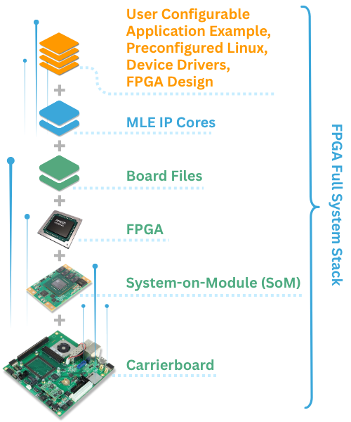
FPGA Full System Stack

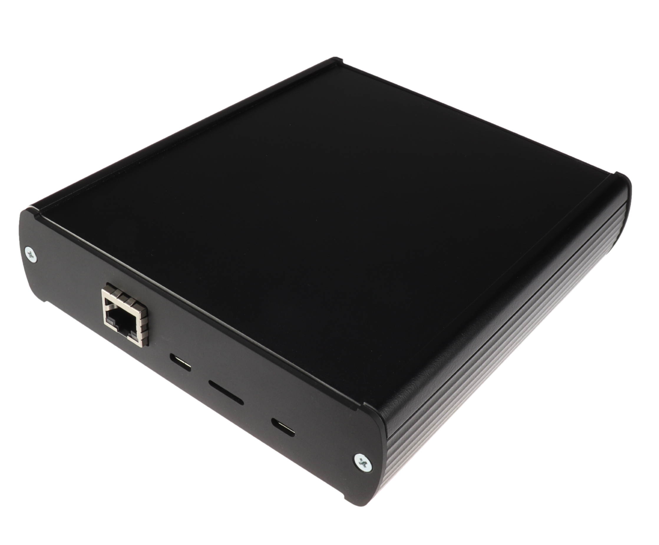
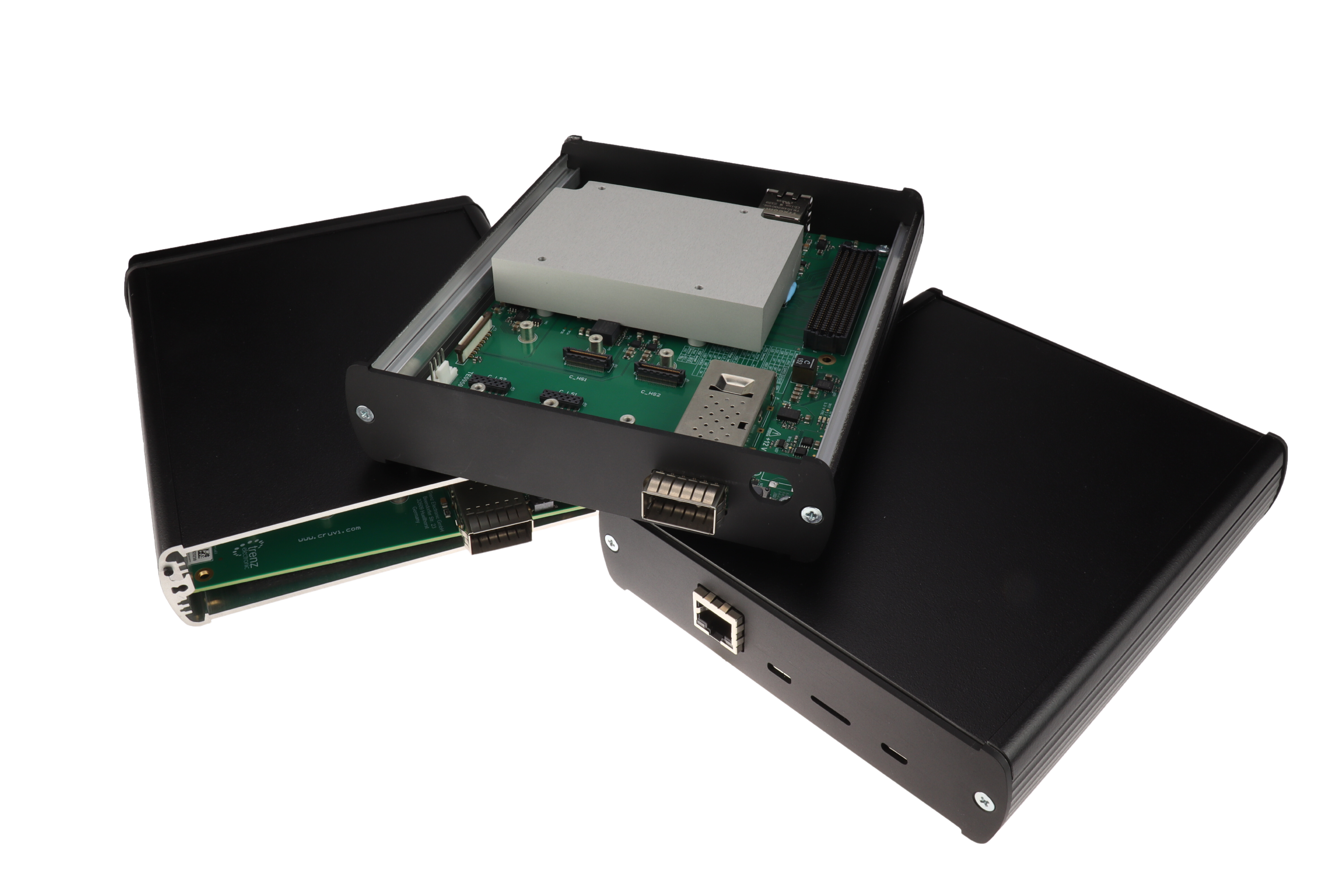
MLE NPAP-25G TCP/UDP/IP Full Accelerator on Trenz Electronics TE0950 Board
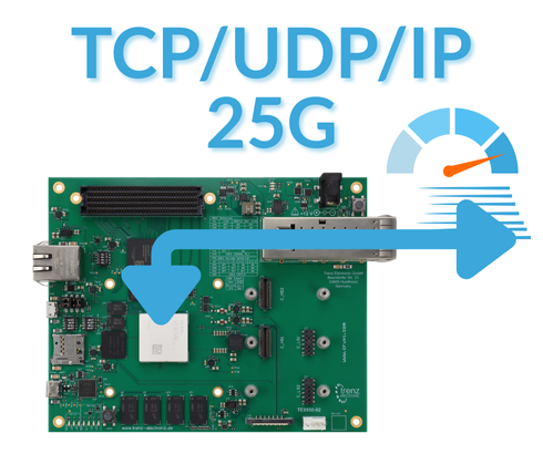
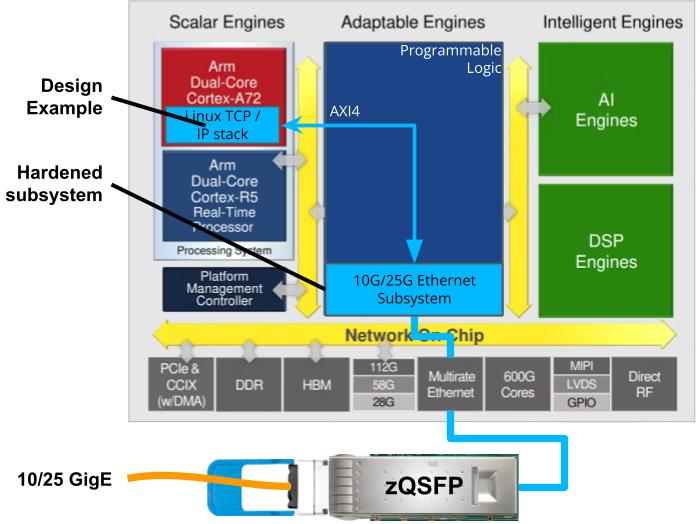
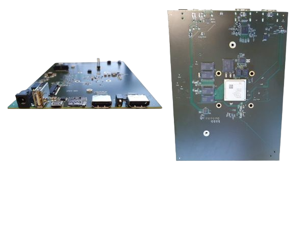
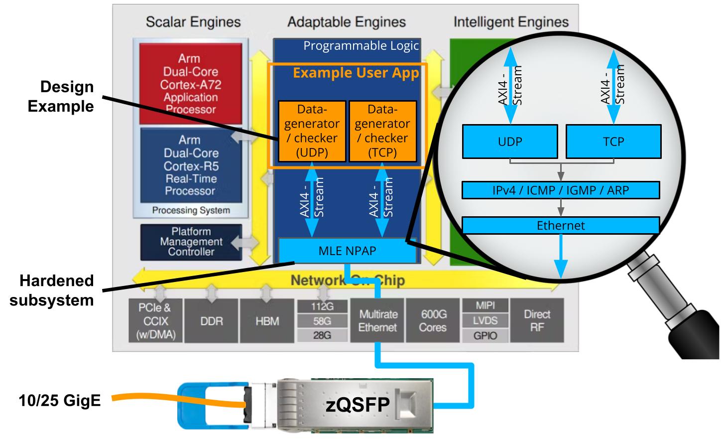 FFSS-TE0950-NPAP-25G Block Diagram | MLE NPAP-25G TCP/UDP/IP Full Accelerator on Trenz Electronics TE0950 BoardMLE NPAP-25G is a full accelerator for 25 GigE network stack based on MLE TCP/UDP/IPv4 Network Protocol Accelerator Platform (NPAP). Trenz TE0950 board is an FPGA Evalboard with AMD Versal™ AI Edge VE2302. The FFSS-TE0950-NPAP-25G is a customizable FPGA design platform with accelerated 25 GigE network connectivity. This FPGA Full Systems Stack combines MLE NPAP with Trenz Electronic’s TE0950 Evaluation Board featuring the AMD Versal™ AI Edge VE2302. All key functionality is pre-integrated and pre-validated and ships as a compilable FPGA design project along with an IP-Core license from MLE. |
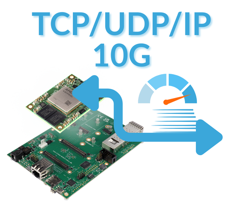
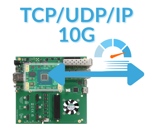
MLE NPAP-10G TCP/UDP/IP Full Accelerator on Trenz Electronics TE0950 Board
FFSS-TE0950-NPAP-10G Block Diagram | MLE NPAP-10G TCP/UDP/IP Full Accelerator on Trenz Electronics TE0950 BoardMLE NPAP-10G is a full accelerator for 10 GigE network stack based on MLE TCP/UDP/IPv4 Network Protocol Accelerator Platform (NPAP). Trenz TE0950 board is an FPGA Evalboard with AMD Versal™ AI Edge VE2302. The FFSS-TE0950-NPAP-10G is a customizable FPGA design platform with accelerated 10 GigE network connectivity. This FPGA Full Systems Stack combines MLE NPAP (the TCP/UDP/IP Network Protocol Acceleration Platform) with Trenz Electronic’s TE0950 Evaluation Board featuring the AMD Versal™ AI Edge VE2302. All key functionality is pre-integrated and pre-validated and ships as a compilable FPGA design project along with an IP-Core license from MLE. |

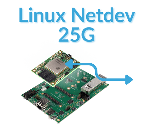
MLE Netdev-25G on Trenz Electronics TE0950 Board
| MLE Netdev-25G on Trenz Electronics TE0950 BoardMLE Netdev-25G is an optimized Linux-based (Non-Accelerated) 25 GigE network stack. Trenz TE0950 board is an FPGA Evalboard with AMD Versal™ AI Edge VE2302. The FFSS-TE0950-Netdev-25G is a customizable FPGA design platform for Linux-based (non-accelerated) 25 GigE network connectivity. This FPGA Full Systems Stack combines an MLE optimized Linux network stack with Trenz Electronic’s TE0950 Evaluation Board featuring the AMD Versal™ AI Edge VE2302. All key functionality is pre-integrated and pre-validated and ships as a compilable FPGA design project along with an IP-Core license from MLE. |
 FFSS-TE0950-Netdev-25G Block Diagram
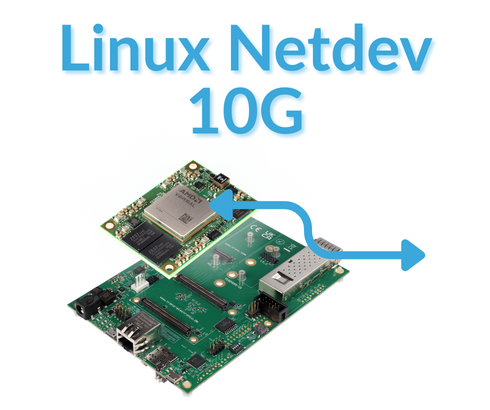
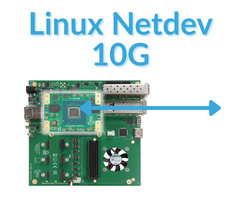
MLE Netdev-10G on Trenz Electronics TE0950 Board
| MLE Netdev-10G on Trenz Electronics TE0950 BoardMLE Netdev-10G is an optimized Linux-based (Non-Accelerated) 10 GigE network stack. Trenz TE0950 board is an FPGA Evalboard with AMD Versal™ AI Edge VE2302. The FFSS-TE0950-Netdev-10G is a customizable FPGA design platform for Linux-based (non-accelerated) 10 GigE network connectivity. This FPGA Full Systems Stack combines an MLE optimized Linux network stack with Trenz Electronic’s TE0950 Evaluation Board featuring the AMD Versal™ AI Edge VE2302. All key functionality is pre-integrated and pre-validated and ships as a compilable FPGA design project along with an IP-Core license from MLE. |
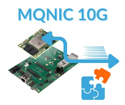
MLE MQNIC-25G on Trenz Electronics TE0950 Board
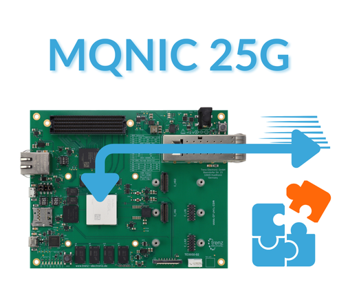 | MLE MQNIC-25G on Trenz Electronics TE0950 BoardMLE MQNIC-25G is a configurable Multi-Queue 25 GigE network stack. Trenz TE0950 board is an FPGA Evalboard with AMD Versal™ AI Edge VE2302. The FFSS-TE0950-MQNIC-25G is a customizable FPGA design platform with configurable Multi-Queue 25 GigE network connectivity. This FPGA Full Systems Stack combines an MLE optimized Linux network stack with Trenz Electronic’s TE0950 Evaluation Board featuring the AMD Versal™ AI Edge VE2302. All key functionality is pre-integrated and pre-validated and ships as a compilable FPGA design project along with an IP-Core license from MLE. |
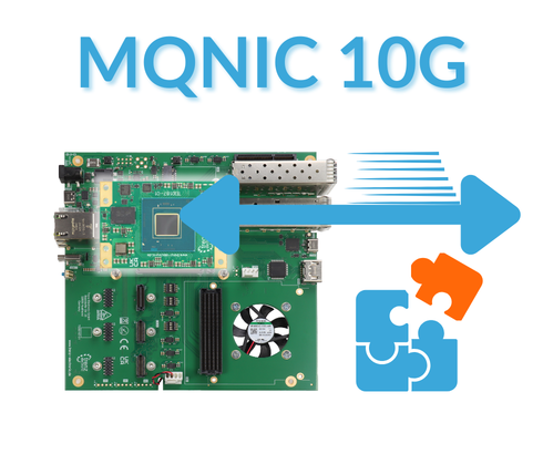
MLE MQNIC-10G on Trenz Electronics TE0950 Board
 | MLE MQNIC-10G on Trenz Electronics TE0950 BoardMLE MQNIC-10G is a configurable Multi-Queue 10 GigE network stack. Trenz TE0950 board is an FPGA Evalboard with AMD Versal™ AI Edge VE2302. The FFSS-TE0950-MQNIC-10G is a customizable FPGA design platform with configurable Multi-Queue 10 GigE network connectivity. This FPGA Full Systems Stack combines an MLE optimized Linux network stack with Trenz Electronic’s TE0950 Evaluation Board featuring the AMD Versal™ AI Edge VE2302. All key functionality is pre-integrated and pre-validated and ships as a compilable FPGA design project along with an IP-Core license from MLE. |
MLE NPAP-25G TCP/UDP/IP Full Accelerator on Trenz Electronics TE0955 Board
FFSS-TE0955-NPAP-25G Block Diagram | MLE NPAP-25G TCP/UDP/IP Full Accelerator on Trenz Electronics TE0955 BoardMLE NPAP-25G is a full accelerator for 25 GigE network stack based on MLE TCP/UDP/IPv4 Network Protocol Accelerator Platform (NPAP). Trenz TE0955 is an FPGA System-on-Module with AMD Versal™ AI Edge VE2302 compatible with TEB0955 Carrierboard. The FFSS-TE0955-NPAP-25G is a customizable FPGA design platform with accelerated 25 GigE network connectivity. This FPGA Full Systems Stack combines MLE NPAP (the TCP/UDP/IP Network Protocol Acceleration Platform) with Trenz Electronic’s TE0955 System-on-Module featuring the AMD Versal™ AI Edge VE2302 and TEB0955 Carrierboard. All key functionality is pre-integrated and pre-validated and ships as a compilable FPGA design project along with an IP-Core license from MLE. |

MLE NPAP-10G TCP/UDP/IP Full Accelerator on Trenz Electronics TE0955 Board
FFSS-TE0955-NPAP-10G Block Diagram | MLE NPAP-10G TCP/UDP/IP Full Accelerator on Trenz Electronics TE0955 BoardMLE NPAP-10G is a full accelerator for 10 GigE network stack based on MLE TCP/UDP/IPv4 Network Protocol Accelerator Platform (NPAP). Trenz TE0955 is an FPGA System-on-Module with AMD Versal™ AI Edge VE2302 compatible with TEB0955 Carrierboard. The FFSS-TE0955-NPAP-10G is a customizable FPGA design platform with accelerated 10 GigE network connectivity. This FPGA Full Systems Stack combines MLE NPAP (the TCP/UDP/IP Network Protocol Acceleration Platform) with Trenz Electronic’s TE0955 System-on-Module featuring the AMD Versal™ AI Edge VE2302 and TEB0955 Carrierboard. All key functionality is pre-integrated and pre-validated and ships as a compilable FPGA design project along with an IP-Core license from MLE. |
MLE Netdev-25G on Trenz Electronics TE0955 Board
FFSS-TE0955-Netdev-25G Block Diagram | MLE Netdev-25G on Trenz Electronics TE0955 BoardMLE Netdev-25G is an optimized Linux-based (Non-Accelerated) 25 GigE network stack. Trenz TE0955 is an FPGA System-on-Module with AMD Versal™ AI Edge VE2302 compatible with TEB0955 Carrierboard. The FFSS-TE0955-Netdev-25G is a customizable FPGA design platform for Linux-based (non-accelerated) 25 GigE network connectivity. This FPGA Full Systems Stack combines an MLE optimized Linux network stack with Trenz Electronic’s TE0955 System-on-Module featuring the AMD Versal™ AI Edge VE2302 and TEB0955 Carrierboard. All key functionality is pre-integrated and pre-validated and ships as a compilable FPGA design project along with an IP-Core license from MLE. |
MLE Netdev-10G on Trenz Electronics TE0955 Board
FFSS-TE0955-Netdev-10G Block Diagram | MLE Netdev-10G on Trenz Electronics TE0955 BoardMLE Netdev-10G is an optimized Linux-based (Non-Accelerated) 10 GigE network stack. Trenz TE0955 is an FPGA System-on-Module with AMD Versal™ AI Edge VE2302 compatible with TEB0955 Carrierboard. The FFSS-TE0955-Netdev-10G is a customizable FPGA design platform for Linux-based (non-accelerated) 10 GigE network connectivity. This FPGA Full Systems Stack combines an MLE optimized Linux network stack with Trenz Electronic’s TE0955 System-on-Module featuring the AMD Versal™ AI Edge VE2302 and TEB0955 Carrierboard. All key functionality is pre-integrated and pre-validated and ships as a compilable FPGA design project along with an IP-Core license from MLE. |
MLE MQNIC-25G on Trenz Electronics TE0955 Board
 | MLE MQNIC-25G on Trenz Electronics TE0955 BoardMLE MQNIC-25G is a configurable Multi-Queue 25 GigE network stack. Trenz TE0955 is an FPGA System-on-Module with AMD Versal™ AI Edge VE2302 compatible with TEB0955 Carrierboard. The FFSS-TE0955-MQNIC-25G is a customizable FPGA design platform with configurable Multi-Queue 25 GigE network connectivity. This FPGA Full Systems Stack combines an MLE optimized Linux network stack with Trenz Electronic’s TE0955 System-on-Module featuring the AMD Versal™ AI Edge VE2302 and TEB0955 Carrierboard. All key functionality is pre-integrated and pre-validated and ships as a compilable FPGA design project along with an IP-Core license from MLE. |
MLE MQNIC-10G on Trenz Electronics TE0955 Board
 | MLE MQNIC-10G on Trenz Electronics TE0955 BoardMLE MQNIC-10G is a configurable Multi-Queue 10 GigE network stack. Trenz TE0955 is an FPGA System-on-Module with AMD Versal™ AI Edge VE2302 compatible with TEB0955 Carrierboard. The FFSS-TE0955-MQNIC-10G is a customizable FPGA design platform with configurable Multi-Queue 10 GigE network connectivity. This FPGA Full Systems Stack combines an MLE optimized Linux network stack with Trenz Electronic’s TE0955 System-on-Module featuring the AMD Versal™ AI Edge VE2302 and TEB0955 Carrierboard. All key functionality is pre-integrated and pre-validated and ships as a compilable FPGA design project along with an IP-Core license from MLE. |
MLE NPAP-25G TCP/UDP/IP Full Accelerator on Trenz Electronics TEI0187 Board
| MLE NPAP-25G TCP/UDP/IP Full Accelerator on Trenz Electronics TEI0187 BoardMLE NPAP-25G is a full accelerator for 25 GigE network stack based on MLE TCP/UDP/IPv4 Network Protocol Accelerator Platform (NPAP). Trenz TEI0187 is an FPGA System-on-Module with Altera® Agilex™ 5E compatible with TEB0187 Carrierboard. The FFSS-TEI0187-NPAP-25G is a customizable FPGA design platform with accelerated 25 GigE network connectivity. This FPGA Full Systems Stack combines MLE NPAP (the TCP/UDP/IP Network Protocol Acceleration Platform) with Trenz Electronic’s TEI0187 System-on-Module featuring the Altera® Agilex™ 5E and TEB0187 Carrierboard. All key functionality is pre-integrated and pre-validated and ships as a compilable FPGA design project along with an IP-Core license from MLE. |
MLE NPAP-10G TCP/UDP/IP Full Accelerator on Trenz Electronics TEI0187 Board
| MLE NPAP-10G TCP/UDP/IP Full Accelerator on Trenz Electronics TEI0187 BoardMLE NPAP-10G is a full accelerator for 10 GigE network stack based on MLE TCP/UDP/IPv4 Network Protocol Accelerator Platform (NPAP). Trenz TEI0187 is an FPGA System-on-Module with Altera® Agilex™ 5E compatible with TEB0187 Carrierboard. The FFSS-TEI0187-NPAP-10G is a customizable FPGA design platform with accelerated 10 GigE network connectivity. This FPGA Full Systems Stack combines MLE NPAP (the TCP/UDP/IP Network Protocol Acceleration Platform) with Trenz Electronic’s TEI0187 System-on-Module featuring the Altera® Agilex™ 5E and TEB0187 Carrierboard. All key functionality is pre-integrated and pre-validated and ships as a compilable FPGA design project along with an IP-Core license from MLE. |
MLE Netdev-25G on Trenz Electronics TEI0187 Board
| MLE Netdev-25G on Trenz Electronics TEI0187 BoardMLE Netdev-25G is an optimized Linux-based (Non-Accelerated) 25 GigE network stack. Trenz TEI0187 is an FPGA System-on-Module with Altera® Agilex™ 5E compatible with TEB0187 Carrierboard. The FFSS-TEI0187-Netdev-25G is a customizable FPGA design platform for Linux-based (non-accelerated) 25 GigE network connectivity. This FPGA Full Systems Stack combines an MLE optimized Linux network stack with Trenz Electronic’s TEI0187 System-on-Module featuring the Altera® Agilex™ 5E and TEB0187 Carrierboard. All key functionality is pre-integrated and pre-validated and ships as a compilable FPGA design project along with an IP-Core license from MLE. |

MLE Netdev-10G on Trenz Electronics TEI0187 Board
| MLE Netdev-10G on Trenz Electronics TEI0187 BoardMLE Netdev-10G is an optimized Linux-based (Non-Accelerated) 10 GigE network stack. Trenz TEI0187 is an FPGA System-on-Module with Altera® Agilex™ 5E compatible with TEB0187 Carrierboard. The FFSS-TEI0187-Netdev-10G is a customizable FPGA design platform for Linux-based (non-accelerated) 10 GigE network connectivity. This FPGA Full Systems Stack combines an MLE optimized Linux network stack with Trenz Electronic’s TEI0187 System-on-Module featuring the Altera® Agilex™ 5E and TEB0187 Carrierboard. All key functionality is pre-integrated and pre-validated and ships as a compilable FPGA design project along with an IP-Core license from MLE. |
MLE MQNIC-25G on Trenz Electronics TEI0187 Board
 | MLE MQNIC-25G on Trenz Electronics TEI0187 BoardMLE MQNIC-25G is a configurable Multi-Queue 25 GigE network stack. Trenz TEI0187 is an FPGA System-on-Module with Altera® Agilex™ 5E compatible with TEB0187 Carrierboard. The FFSS-TEI0187-MQNIC-25G is a customizable FPGA design platform with configurable Multi-Queue 25 GigE network connectivity. This FPGA Full Systems Stack combines an MLE optimized Linux network stack with Trenz Electronic’s TEI0187 System-on-Module featuring the Altera® Agilex™ 5E and TEB0187 Carrierboard. All key functionality is pre-integrated and pre-validated and ships as a compilable FPGA design project along with an IP-Core license from MLE. |
MLE MQNIC-10G on Trenz Electronics TEI0187 Board
 | MLE MQNIC-10G on Trenz Electronics TEI0187 BoardMLE MQNIC-10G is a configurable Multi-Queue 10 GigE network stack. Trenz TEI0187 is an FPGA System-on-Module with Altera® Agilex™ 5E compatible with TEB0187 Carrierboard. The FFSS-TEI0187-MQNIC-10G is a customizable FPGA design platform with configurable Multi-Queue 10 GigE network connectivity. This FPGA Full Systems Stack combines an MLE optimized Linux network stack with Trenz Electronic’s TEI0187 System-on-Module featuring the Altera® Agilex™ 5E and TEB0187 Carrierboard. All key functionality is pre-integrated and pre-validated and ships as a compilable FPGA design project along with an IP-Core license from MLE. |
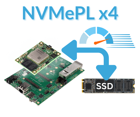
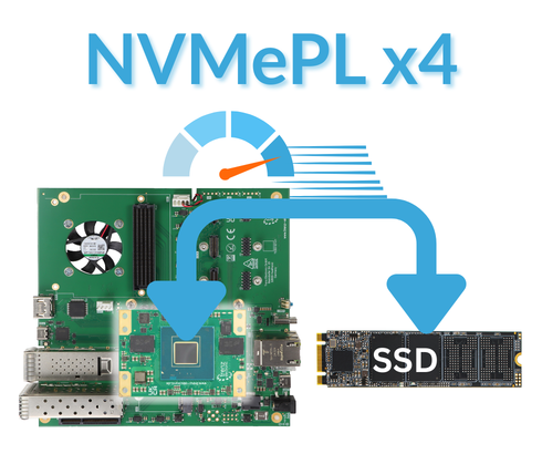
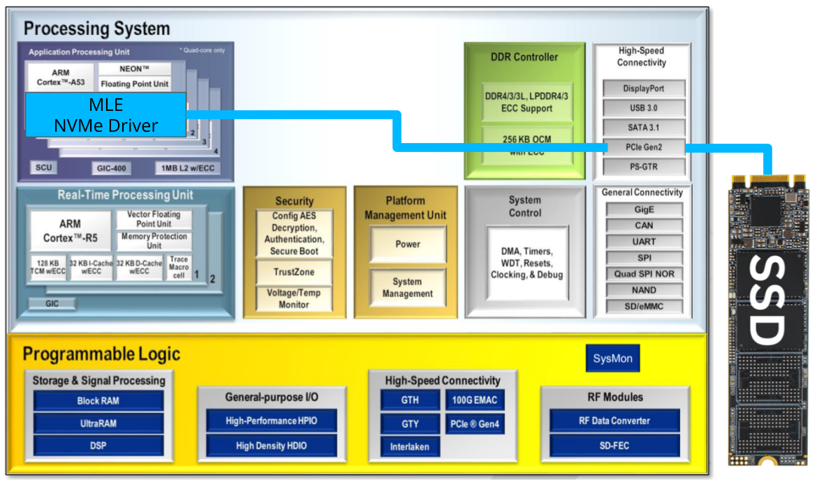
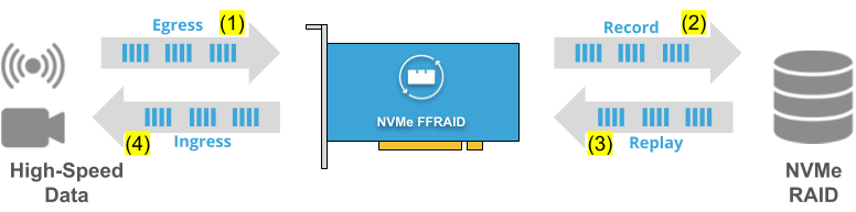
MLE NVMePL-x4 on Trenz Electronics TE0950 Board
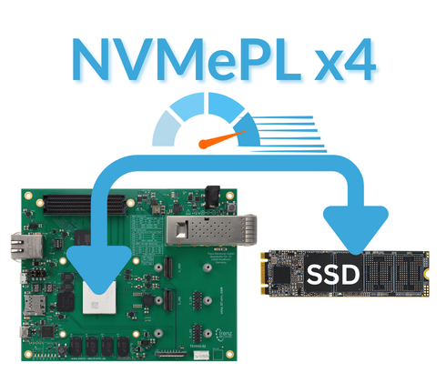 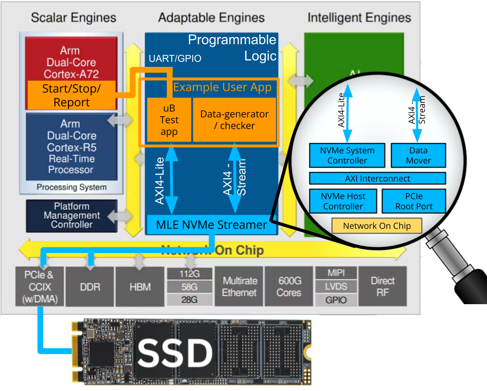 FFSS-TE0950-NVMePL-x4 Block Diagram | MLE NVMePL-x4 on Trenz Electronics TE0950 BoardMLE NVMePL-x4 is a full accelerator for NVMe data streaming with 4 lanes in PL based on MLE NVMe Streamer. Trenz TE0950 board is an FPGA Evalboard with AMD Versal™ AI Edge VE2302. The FFSS-TE0950-NVMePL-x4 is a customizable FPGA design platform with accelerated NVMe data streaming. This FPGA Full Systems Stack combines MLE NVMe Streamer with Trenz Electronic’s TE0950 Evaluation Board featuring the AMD Versal™ AI Edge VE2302. All key functionality is pre-integrated and pre-validated and ships as a compilable FPGA design project along with an IP-Core license from MLE. |
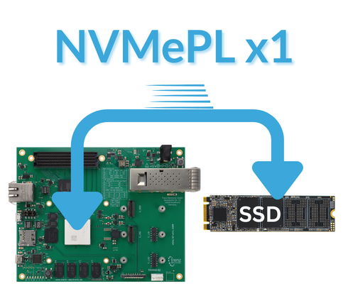
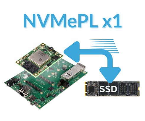
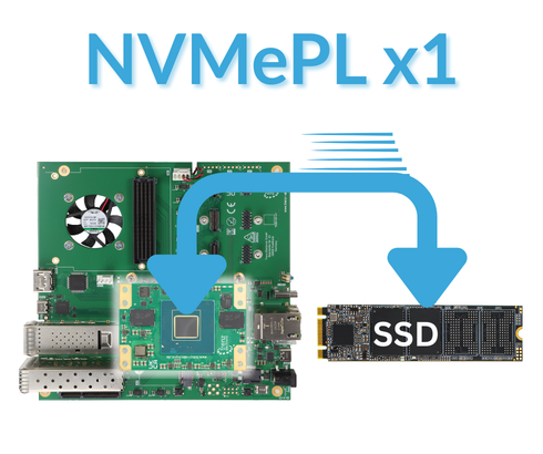
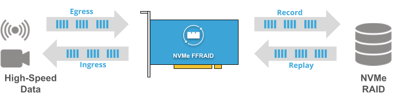
MLE NVMePL-x1 on Trenz Electronics TE0950 Board
FFSS-TE0950-NVMePL-x1 Block Diagram | MLE NVMePL-x1 on Trenz Electronics TE0950 BoardMLE NVMePL-x1 is a full accelerator for NVMe data streaming with 1 lane in PL based on MLE NVMe Streamer. Trenz TE0950 board is an FPGA Evalboard with AMD Versal™ AI Edge VE2302. The FFSS-TE0950-NVMePL-x1 is a customizable FPGA design platform with accelerated NVMe data streaming. This FPGA Full Systems Stack combines MLE NVMe Streamer with Trenz Electronic’s TE0950 Evaluation Board featuring the AMD Versal™ AI Edge VE2302. All key functionality is pre-integrated and pre-validated and ships as a compilable FPGA design project along with an IP-Core license from MLE. |
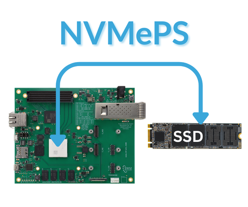
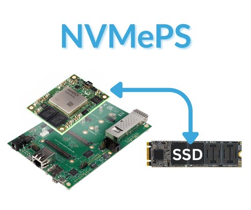
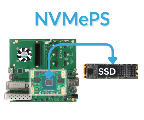
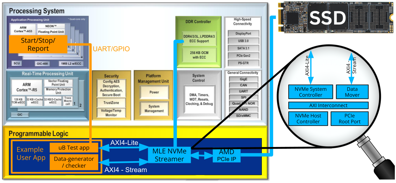
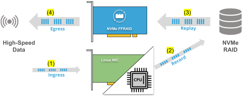
MLE NVMePS on Trenz Electronics TE0950 Board
 FFSS-TE0950-NVMePS Block Diagram | MLE NVMePS on Trenz Electronics TE0950 BoardMLE NVMePS is a storage stack to read/write data onto a Linux-connected NVMe SSD using Linux file system. Trenz TE0950 board is an FPGA Evalboard with AMD Versal™ AI Edge VE2302. The FFSS-TE0950-NVMePS is a customizable FPGA design platform with PS-based NVMe data streaming. This FPGA Full Systems Stack combines MLE Linux-based storage stack with Trenz Electronic’s TE0950 Evaluation Board featuring the AMD Versal™ AI Edge VE2302. All key functionality is pre-integrated and pre-validated and ships as a compilable FPGA design project along with an IP-Core license from MLE. |
MLE NVMePL-x4 on Trenz Electronics TE0955 Board
 FFSS-TE0955-NVMePL-x4 Block Diagram | MLE NVMePL-x4 on Trenz Electronics TE0955 BoardMLE NVMePL-x4 is a full accelerator for NVMe data streaming with 4 lanes in PL based on MLE NVMe Streamer. Trenz TE0955 is an FPGA System-on-Module with AMD Versal™ AI Edge VE2302 compatible with TEB0955 Carrierboard. The FFSS-TE0955-NVMePL-x4 is a customizable FPGA design platform with accelerated NVMe data streaming. This FPGA Full Systems Stack combines MLE NVMe Streamer with Trenz Electronic’s TE0955 System-on-Module featuring the AMD Versal™ AI Edge VE2302 and TEB0955 Carrierboard. All key functionality is pre-integrated and pre-validated and ships as a compilable FPGA design project along with an IP-Core license from MLE. |
MLE NVMePL-x1 on Trenz Electronics TE0955 Board
FFSS-TE0955-NVMePL-x1 Block Diagram | MLE NVMePL-x1 on Trenz Electronics TE0955 BoardMLE NVMePL-x1 is a full accelerator for NVMe data streaming with 1 lane in PL based on MLE NVMe Streamer. Trenz TE0955 is an FPGA System-on-Module with AMD Versal™ AI Edge VE2302 compatible with TEB0955 Carrierboard. The FFSS-TE0955-NVMePL-x1 is a customizable FPGA design platform with accelerated NVMe data streaming. This FPGA Full Systems Stack combines MLE NVMe Streamer with Trenz Electronic’s TE0955 System-on-Module featuring the AMD Versal™ AI Edge VE2302 and TEB0955 Carrierboard. All key functionality is pre-integrated and pre-validated and ships as a compilable FPGA design project along with an IP-Core license from MLE. |
MLE NVMePS on Trenz Electronics TE0955 Board
FFSS-TE0955-NVMePS Block Diagram | MLE NVMePS on Trenz Electronics TE0955 BoardMLE NVMePS is a storage stack to read/write data onto a Linux-connected NVMe SSD using Linux file system. Trenz TE0955 is an FPGA System-on-Module with AMD Versal™ AI Edge VE2302 compatible with TEB0955 Carrierboard. The FFSS-TE0955-NVMePS is a customizable FPGA design platform with PS-based NVMe data streaming. This FPGA Full Systems Stack combines MLE’s Linux-based storage stack with Trenz Electronic’s TE0955 System-on-Module featuring the AMD Versal™ AI Edge VE2302 and TEB0955 Carrierboard. All key functionality is pre-integrated and pre-validated and ships as a compilable FPGA design project along with an IP-Core license from MLE. |
MLE NVMePL-x4 on Trenz Electronics TEI0187 Board
 | MLE NVMePL-x4 on Trenz Electronics TEI0187 BoardMLE NVMePL-x4 is a full accelerator for NVMe data streaming with 4 lanes in PL based on MLE NVMe Streamer. Trenz TEI0187 is an FPGA System-on-Module with Altera® Agilex™ 5E compatible with TEB0187 Carrierboard. The FFSS-TEI0187-NVMePL-x4 is a customizable FPGA design platform with accelerated NVMe data streaming. This FPGA Full Systems Stack combines MLE NVMe Streamer with Trenz Electronic’s TEI0187 System-on-Module featuring the Altera® Agilex™ 5E and TEB0187 Carrierboard. All key functionality is pre-integrated and pre-validated and ships as a compilable FPGA design project along with an IP-Core license from MLE. |
MLE NVMePL-x1 on Trenz Electronics TEI0187 Board
| MLE NVMePL-x1 on Trenz Electronics TEI0187 BoardMLE NVMePL-x1 is a full accelerator for NVMe data streaming with 1 lane in PL based on MLE NVMe Streamer. Trenz TEI0187 is an FPGA System-on-Module with Altera® Agilex™ 5E compatible with TEB0187 Carrierboard. The FFSS-TEI0187-NVMePL-x1 is a customizable FPGA design platform with accelerated NVMe data streaming. This FPGA Full Systems Stack combines MLE NVMe Streamer with Trenz Electronic’s TEI0187 System-on-Module featuring the Altera® Agilex™ 5E and TEB0187 Carrierboard. All key functionality is pre-integrated and pre-validated and ships as a compilable FPGA design project along with an IP-Core license from MLE. |
MLE NVMePS on Trenz Electronics TEI0187 Board
| MLE NVMePS on Trenz Electronics TEI0187 BoardMLE NVMePS is a storage stack to read/write data onto a Linux-connected NVMe SSD using Linux file system. Trenz TEI0187 is an FPGA System-on-Module with Altera® Agilex™ 5E compatible with TEB0187 Carrierboard. The FFSS-TEI0187-NVMePS is a customizable FPGA design platform with PS-based NVMe data streaming. This FPGA Full Systems Stack combines MLE’s Linux-based storage stack with Trenz Electronic’s TEI0187 System-on-Module featuring the Altera® Agilex™ 5E and TEB0187 Carrierboard. All key functionality is pre-integrated and pre-validated and ships as a compilable FPGA design project along with an IP-Core license from MLE. |
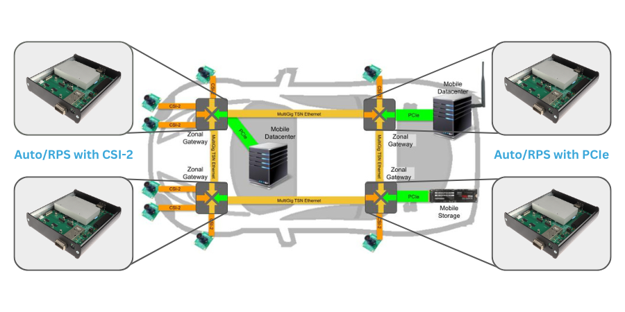
MLE NVMePL-x4 on Alpha Data ADA-VA330 Board
FFSS-ADA-VA330-NVMePL-x4 Block Diagram | MLE NVMePL-x4 on Alpha Data ADA-VA330 BoardMLE NVMePL-x4 is a full accelerator for NVMe data streaming with 4 lanes in PL based on MLE NVMe Streamer. Alpha Data’s ADA-VA330 board is an 14.6.11 SOSA-Aligned 3U VPX Versal™ RF module with AMD Versal™ RF VR1602. The FFSS-ADA-VA330-NVMePL-x4 combines MLE’s NVMe Streamer Subsystems with Alpha Data’s ADA-VA330 board featuring the AMD Versal™ RF VR1602 for 16 DACs and 16 ADCs at 14-bit resolution with up to 18GHz bandwidth combined with powerful hardened IP for FFT, channelization, LDPC decode, and resample. All key functionality is pre-integrated and pre-validated and ships as a compilable FPGA design project along with an IP-Core license from MLE. The FFSS-ADA-VA330-NVMePL-x4 comprehensively manages the data path, configuring the PCIe core for high-speed transfer. |
MLE NVMePL-x1 on Alpha Data ADA-VA330 Board
FFSS-ADA-VA330-NVMePL-x1 Block Diagram | MLE NVMePL-x1 on Alpha Data ADA-VA330 BoardMLE NVMePL-x1 is a full accelerator for NVMe data streaming with 1 lane in PL based on MLE NVMe Streamer. Alpha Data’s ADA-VA330 board is an 14.6.11 SOSA-Aligned 3U VPX Versal™ RF module with AMD Versal™ RF VR1602. The FFSS-ADA-VA330-NVMePL-x1 combines MLE’s NVMe Streamer Subsystems with Alpha Data’s ADA-VA330 board featuring the AMD Versal™ RF VR1602 for 16 DACs and 16 ADCs at 14-bit resolution with up to 18GHz bandwidth combined with powerful hardened IP for FFT, channelization, LDPC decode, and resample. All key functionality is pre-integrated and pre-validated and ships as a compilable FPGA design project along with an IP-Core license from MLE. The FFSS-ADA-VA330-NVMePL-x4 comprehensively manages the data path, configuring the PCIe core for high-speed transfer. |
MLE NVMePS on Alpha Data ADA-VA330 Board
 FFSS-ADA-VA330-NVMePS Block Diagram | MLE NVMePS on Alpha Data ADA-VA330 BoardMLE NVMePS is a storage stack to read/write data onto a Linux-connected NVMe SSD using Linux file system. Alpha Data’s ADA-VA330 board is an 14.6.11 SOSA-Aligned 3U VPX Versal™ RF module with AMD Versal™ RF VR1602. The FFSS-ADA-VA330-NVMePS combines MLE’s Linux-based storage stack with Alpha Data’s ADA-VA330 board featuring the AMD Versal™ RF VR1602 for 16 DACs and 16 ADCs at 14-bit resolution with up to 18GHz bandwidth combined with powerful hardened IP for FFT, channelization, LDPC decode, and resample. All key functionality is pre-integrated and pre-validated and ships as a compilable FPGA design project along with an IP-Core license from MLE. The FFSS-ADA-VA330-NVMePS manages the data path, configuring the PCIe core for high-speed transfer. |
MLE NVMePL-x4 on Alpha Data ADA-V9202 Board
 FFSS-ADA-V9202-NVMePL-x4 Block Diagram | MLE NVMePL-x4 on Alpha Data ADA-V9202 BoardMLE NVMePL-x4 is a full accelerator for NVMe data streaming with 4 lanes in PL based on MLE NVMe Streamer. Alpha Data’s ADA-V9202 board is a SOSA-Aligned 3U VPX module with AMD Zynq® Ultrascale+ XCZU47DR-2 or XCZU48DR-2 (FFVE1156). The FFSS-ADA-V9202-NVMePL-x4 combines MLE’s NVMe Streamer Subsystems with Alpha Data’s ADA-V9202 rugged SOSA-Aligned 3U VPX format module and is available in industrial temperature grades with conduction cooling. All key functionality is pre-integrated and pre-validated and ships as a compilable FPGA design project along with an IP-Core license from MLE. The FFSS-ADA-V9202-NVMePL-x4 comprehensively manages the data path, configuring the PCIe core for high-speed transfer. |
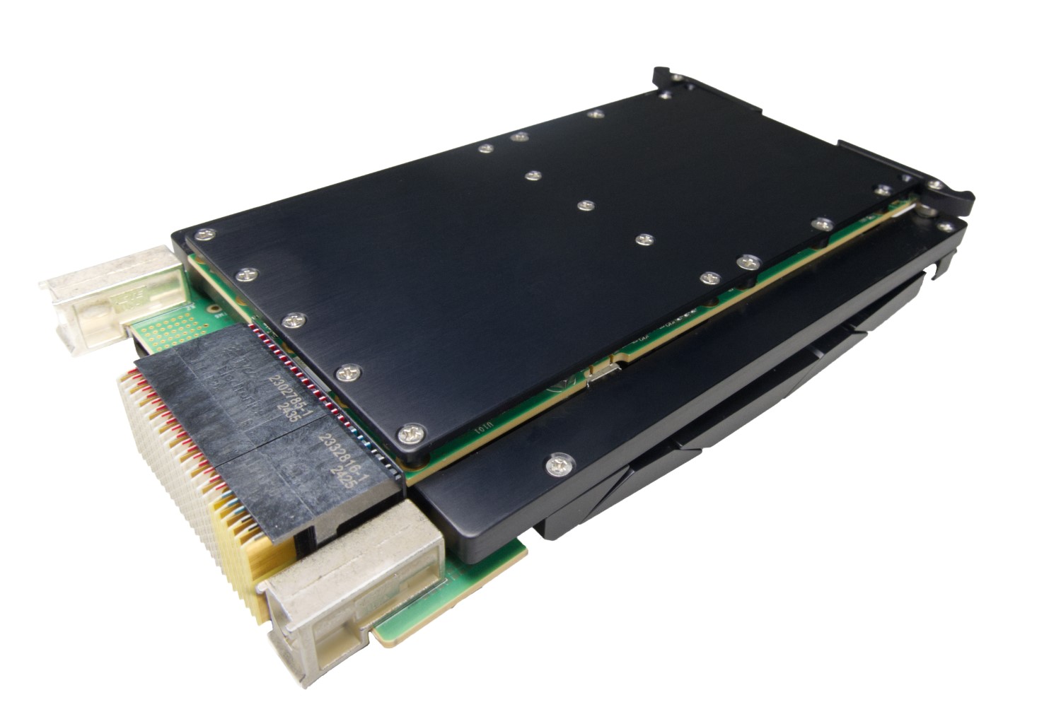
MLE NVMePL-x1 on Alpha Data ADA-V9202 Board
FFSS-ADA-V9202-NVMePL-x1 Block Diagram | MLE NVMePL-x1 on Alpha Data ADA-V9202 BoardMLE NVMePL-x1 is a full accelerator for NVMe data streaming with 1 lane in PL based on MLE NVMe Streamer. Alpha Data’s ADA-V9202 board is a SOSA-Aligned 3U VPX module with AMD Zynq® Ultrascale+ XCZU47DR-2 or XCZU48DR-2 (FFVE1156). The FFSS-ADA-V9202-NVMePL-x1 combines MLE’s NVMe Streamer Subsystems with Alpha Data’s ADA-V9202 rugged SOSA-Aligned 3U VPX format module and is available in industrial temperature grades with conduction cooling. All key functionality is pre-integrated and pre-validated and ships as a compilable FPGA design project along with an IP-Core license from MLE. The FFSS-ADA-V9202-NVMePL-x1 comprehensively manages the data path, configuring the PCIe core for high-speed transfer. |
MLE NVMePS on Alpha Data ADA-V9202 Board
 FFSS-ADA-V9202-NVMePS Block Diagram | MLE NVMePS on Alpha Data ADA-V9202 BoardMLE NVMePS is a storage stack to read/write data onto a Linux-connected NVMe SSD using Linux file system. Alpha Data’s ADA-V9202 board is a SOSA-Aligned 3U VPX module with AMD Zynq® Ultrascale+ XCZU47DR-2 or XCZU48DR-2 (FFVE1156). The FFSS-ADA-V9202-NVMS combines MLE’s Linux-based storage stack with Alpha Data’s ADA-V9202 rugged SOSA-Aligned 3U VPX format module and is available in industrial temperature grades with conduction cooling. All key functionality is pre-integrated and pre-validated and ships as a compilable FPGA design project along with an IP-Core license from MLE. The FFSS-ADA-V9202-NVMePS manages the data path, configuring the PCIe core for high-speed transfer. |


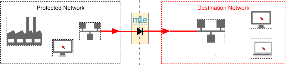
")
")


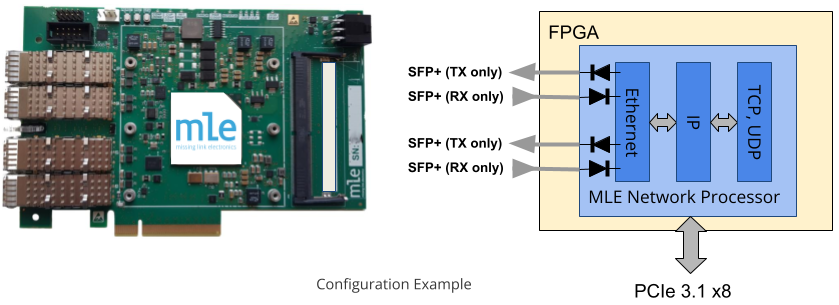


 MLE is a contributor to the Corundum project. Please visit our