As the demand for domain-specific architectures grows, FPGAs have become essential for offloading compute-intensive tasks in networking, storage, and automotive sectors. However, the “Integration Gap”—the months of engineering effort required to build reliable PCIe/DMA infrastructure, kernel drivers, and memory management—often acts as a barrier to entry.
This presentation introduces the Missing Link Electronics (MLE) FPGA Full System Stack (FFSS), a pre-validated, cross-platform framework designed to eliminate architectural “plumbing” and accelerate application-specific development.
Date: Thursday July 2rd, 2026
Track Architecture2:20pm-3:00pm CEST
Location: Hotel NH München East Conference Center, Munich, Germany
Join MLE at FPGA Conference 2026 and discover how our FPGA Full System Stacks de-risk design process, rapidly validate your prototypes, and accelerate your time-to-market!
“When Wall Street Wanted to Program Computers without having computer programmers, they invented the spreadsheet!” This was our spirit when we came up with FPGA Full System Stacks: Make building FPGA-based systems easier for engineers without expert knowledge in FPGA design.
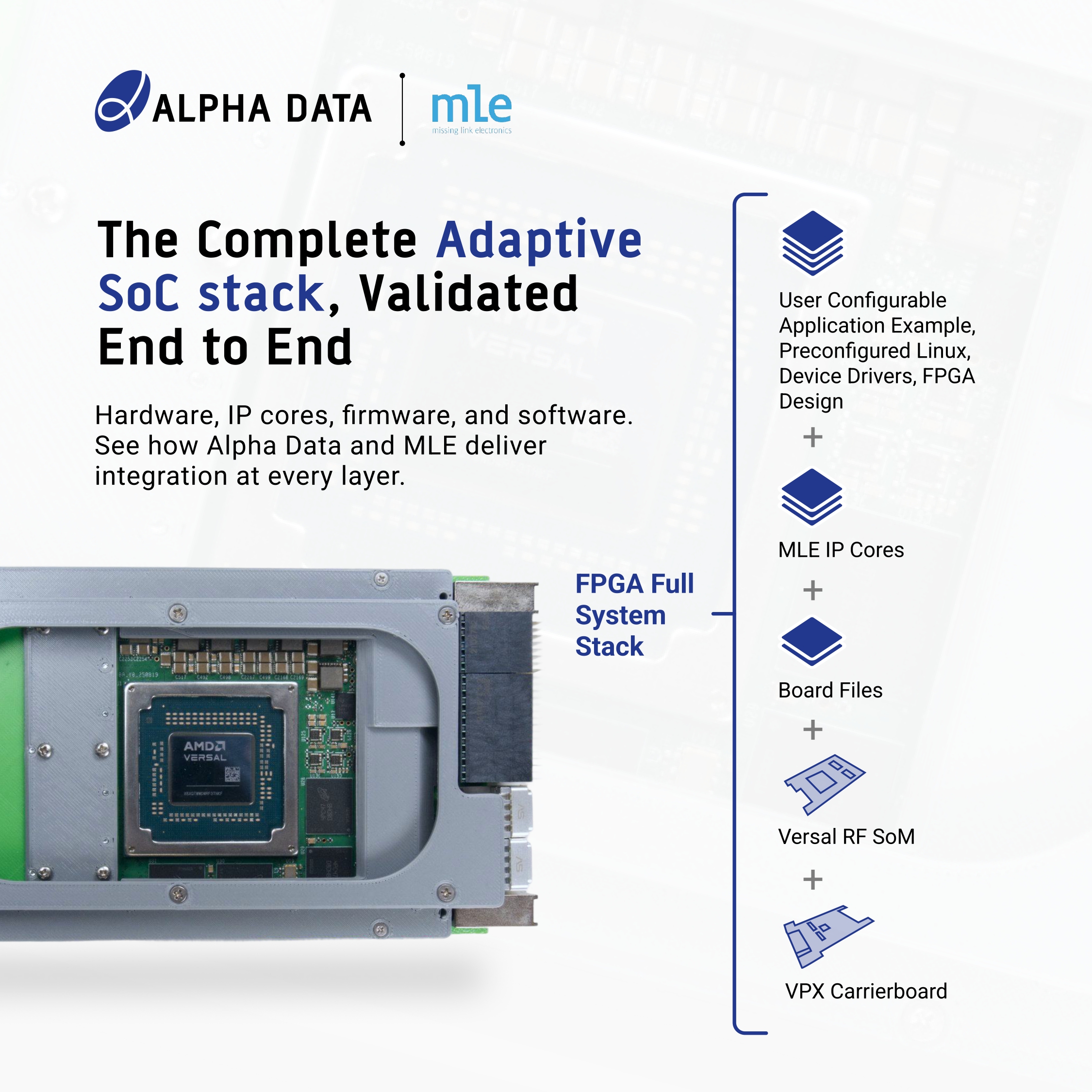
Littleton, CO, June 8, 2026 – Alpha Data Parallel Systems and Missing Link Electronics (MLE) have announced a technology partnership aimed at simplifying FPGA (Field-Programmable Gate Array) deployment for defense and aerospace customers.
The collaboration introduces a new concept “FPGA Full System Stacks”, integrated hardware and software platforms designed to reduce procurement complexity, development risk, and time-to-deployment for FPGA based systems.
The platforms combine Alpha Data’s ruggedized, SOSA (Sensor Open Systems Architecture)-aligned FPGA hardware with MLE’s pre-validated IP cores and software stacks, covering applications including high-speed data recording, signal processing, data transport, and system-level firmware. The result is a fully integrated FPGA platform delivered through a single vendor relationship.
Defense programs often face delays and complexity when procuring FPGA software and specialist IP separately from hardware. The FPGA Full System Stack approach allows customers to source integrated hardware and software through a single approved supplier. Because each platform is validated end-to-end before delivery, customers can reduce qualification overhead, accelerate development timelines, and lower integration risk.
As AMD Premier Partners, both companies bring extensive FPGA expertise to the offering. The collaboration provides customers with a single point of accountability across hardware, software, and overall system performance.
Adam Smith, Chief Executive Officer of Alpha Data, said:
“Defense customers should not have to carry the cost and risk of integrating hardware and software themselves. By partnering with MLE, we’re lifting the procurement burden from our end customers, offering hardware and software that is qualified and procured together, ready to deploy. That is a meaningful change for program teams working under time and budget pressure.”
Endric Schubert, CTO of Missing Link Electronics added:
“The new Alpha Data FPGA Full System Stacks integrates and verifies everything engineers need to develop their application immediately. This eliminates the time and effort required to build a prototype from scratch, enabling teams to validate concepts rapidly. At the same time, this integrated approach ensures the users are fully supported by both hardware and software experts throughout their development cycle.”
The offering targets mission-critical aerospace and defense applications including, radar and sonar systems, electromagnetic spectrum operations (EMSO), military communications using MIMO and pre-6G waveform processing, edge AI inference, and signals intelligence (SIGINT).
The product line also supports space and satellite applications, including hardware configurations with single-event latch-up mitigation for high-radiation environments. Each platform is SOSA-aligned and qualified for deployment in ruggedized, conduction-cooled environments.
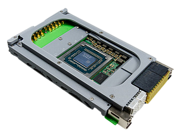
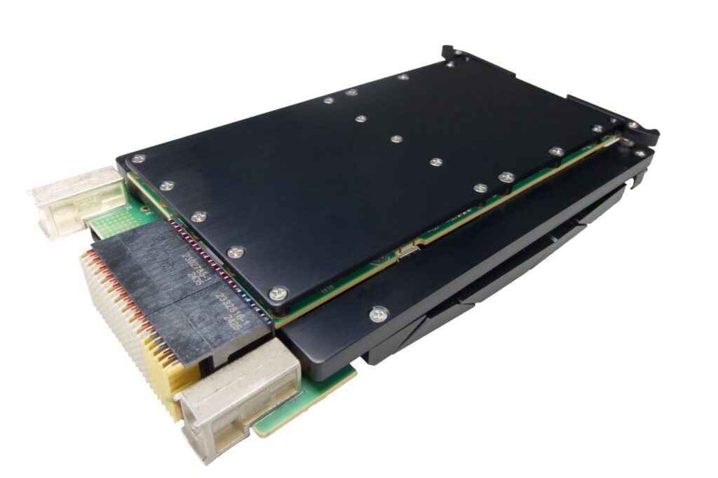
Alpha Data SOSA-aligned FPGA Full System Stack in VPX format
Securing data at the edge requires close alignment between hardware capabilities and trusted software environments. Missing Link Electronics (MLE) has extended the Open Portable Trusted Execution Environment (OP-TEE) to support advanced hardware-accelerated cryptographic capabilities on a high-performance AMD Versal™ Adaptive SoC platform.
This work focuses on integrating key cryptographic primitives directly into the trusted execution environment, enabling efficient and secure access to hardware-backed security features. The implementation includes support for:
SHA2-256, SHA2-384, and SHA2-512 hashing
Counter DRBG (Deterministic Random Bit Generator)
ECDSA Key Generation, Signature Generation, and Verification
By tightly coupling OP-TEE with on-chip cryptographic accelerators, the solution enables high-assurance execution environments suitable for security-sensitive edge deployments.
This work highlights MLE’s capability to deliver secure, hardware-integrated trusted execution environments that support the growing complexity of edge computing systems.
As autonomous driving and advanced driver-assistance systems (ADAS) evolve, modern vehicles require unprecedented levels of environmental awareness to enhance and ensure driving safety. According to the article “High-Precision Synchronization for 77-GHz Radar Networks via White Rabbit” in Journal of IEEE Transactions on Radar Systems, this demand is driving the deployment of distributed 77GHz automotive radar networks, which rely on coherent data processing to create a precise, real-time map of the vehicle’s surroundings. To achieve this, the distributed sensors must be synchronized with sub-nanosecond accuracy. Existing wired synchronization methods, however, incur high cabling costs and present challenges in complexity and scalability.
White Rabbit (WR) Technology, an Ethernet-based technology providing sub-nanosecond accuracy, enables simultaneous synchronization and data transfer over a standard Ethernet link, thus eliminating the need for a dedicated custom clock distribution network. To implement this technology in FPGAs, it typically requires external voltage-controlled crystal oscillators (VCXOs) for measurement and adjustment. However, such components are often missing on commercially off-the-shelf (COTS) development boards. This forces interested developers to invest inexpensive, specialized hardware just to get started with White Rabbit technology.
The Dormouse White Rabbit FPGA FMC features tunable oscillators that are required to deploy and operate White Rabbit, an open-source FPGA-based implementation of Precision Time Protocol 2.1 (PTP v2.1), and provides capabilities to generate LF and RF reference clocks derived from a White Rabbit network. For these tasks a high performance OCXO (DOT050V), two programmable and tunable oscillators (SiT3521, Si549) and a flexible PLL (HMC7044) are available for use on the card.
With the Dormouse White Rabbit FPGA FMC, White Rabbit implementation can achieve < 1 ns accuracy and < 100 ps precision of the PTP v2.1 high-accuracy profile for building a time and frequency distributed 77GHz automotive radar networks.
When Wall Street Wanted to Program Computers without having computer programmers, they invented the spreadsheet!
This was our spirit when we came up with FPGA Full System Stacks: Make building FPGA-based systems easier for engineers without expert knowledge in FPGA design.
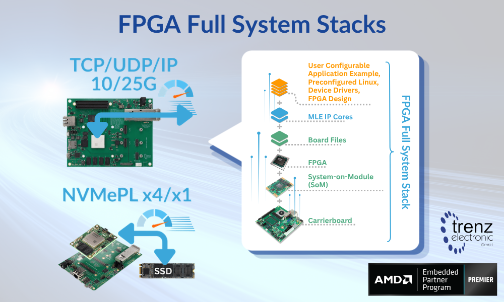
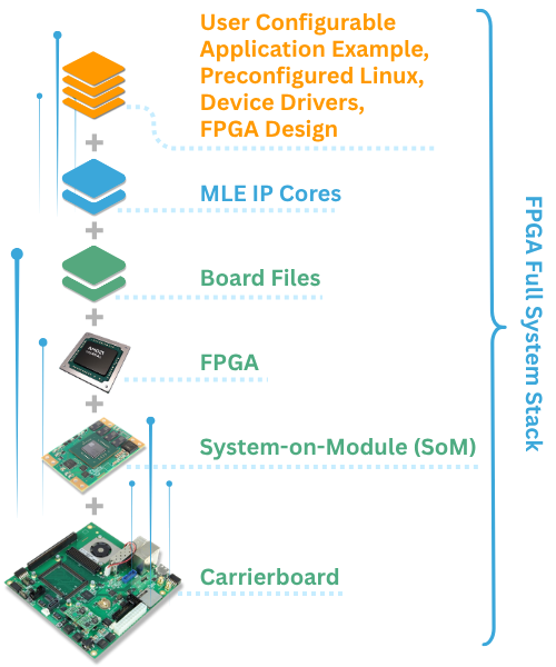
Trenz Electronic and Missing Link Electronics (MLE), both Premier Members of the AMD Embedded Partner Program, today announce the launch of their first set of “FPGA Full System Stacks (FFSS)” for AMD Versal™.
These FPGA Full System Stacks deliver pre-validated, user-customizable building blocks that integrate FPGA hardware along with acceleration subsystems combining different Intellectual Property (IP) cores, which in concert solve the most common performance bottlenecks in Networking, Storage, and Signal Processing.
Besides the concept of pre-validated, user-customizable building blocks, FPGA Full System Stacks also come with a cost-optimized licensing scheme:
While the typical license costs for such IP Cores can run up to $100k (or more, depending on what accelerators you may need), the cost of an FFSS is very compatible with most low-unit-volume FPGA applications, sometimes around the same cost as the hardware itself.
Bridging the Gap in FPGA Accessibility
As Field-Programmable Gate Arrays (FPGAs) continue to dominate sectors such as Automotive, Aerospace, Industrial, and Telecommunications due to their unmatched flexibility and energy efficiency, the barrier to entry remains high. However, the difficulty in programming FPGAs, in particular those System-on-Chip (SoC) FPGA with embedded CPUs, has long been considered a disadvantage that prevents FPGA from becoming a general computation solution.
The concept of FPGA Full System Stack is designed to address this challenge. With MLE FPGA IP Cores pre-integrated and pre-validated on Trenz System-on-Modules (SoMs) and Carrierboards, the solution allows developers to bypass the “ground-up” hardware-software integration phase. Instead, users can immediately focus on application-layer development, significantly increasing productivity while shortening time-to-market for new product initiatives.
FPGA Full System Stacks: Ready-To-Run for Modern Workloads
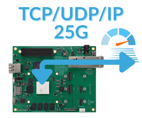
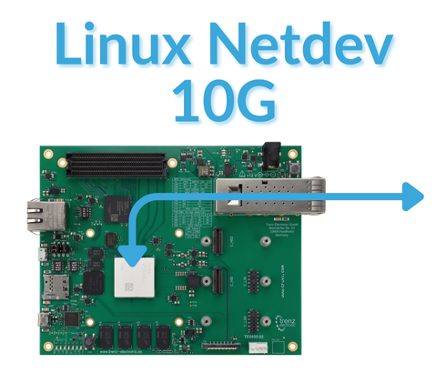
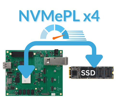
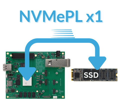
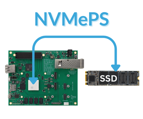
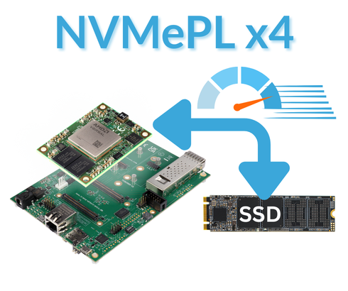
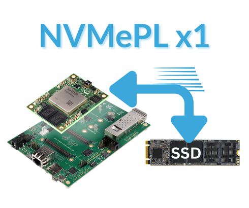
The current portfolio focuses on Compute, Video, Storage and Network Acceleration, leveraging the power of AMD Versal™ AI series on the Trenz TE0950 Evalboard and on the Trenz TE0955 SoM along with the Trenz TEB0955 carrierboard. Key configurations available at launch include:
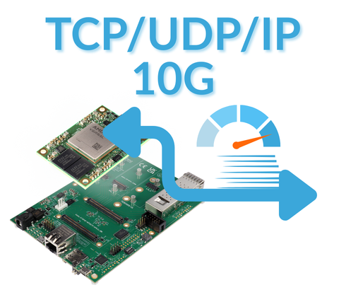
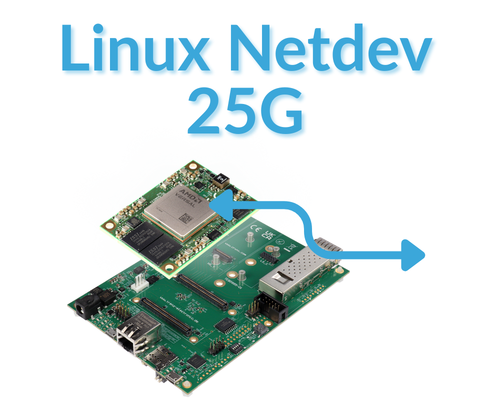
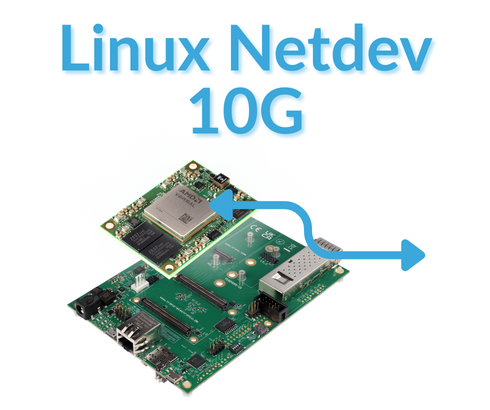
Networking FPGA Full System Stacks for AMD Versal™:
The United States Patent and Trademark Office (USPTO) has issued to Missing Link Electronics, Inc. the US Patent No. 12,592,898 B2 for “Tightly-Coupled, Loosely Connected Heterogeneous Packet Based Transport”, a technology that finds applications in automotive networking, factory automation and robotics, sensor open system architectures, and 5G Radio campus networks.
ADAS with coherent, multi-static, digital RADAR benefits from automotive Ethernet but demands more precise time synchronization and clock-phase recovery.
First we give an overview over time synchronization: NTP, GNSS, PTP, with a deep-dive into the PTP (including hardware assisted time stamping for accuracy and precision around 10 nanoseconds), down to the high-accuracy Precision Time Protocol IEEE 1588-2019 (PTP-HA) developed by CERN’s White Rabbit group for large scale physics experiments in need of < 1 ns accuracy and < 100 ps precision.
Second we present “Light Rabbit”, a collaboration between CERN and MLE. Using modern on-chip PLL for phase-shifting we complement (or replace) expensive VCXOs and trade-off BoM cost vs. minor loss of accuracy.
We close with experimental results for an OFDM RADAR network where Ethernet transports status, control and sensor data and distributes time (i.e. trigger), frequency and phase information to steer oscillators in the RF subsystem.
Date: Thursday March 26, 2026
Session 6 – TSN (starts at 10:30am CEST)
Location: Science Congress Center Munich, Germany
Join us at Automotive Ethernet Congress 2026 to learn more about the “Light Rabbit” solution to complement White Rabbit technology for high-accuracy time synchronization of digital radar networks!
Modern Software-Defined Vehicle (SDV) architectures are pushing automotive in-vehicle networks towards more bandwidth and lower, guaranteed transport latency as cars are expected to be an integral part of a broader software and services eco-system, can be continuously updated/upgraded with new features, and achieve higher levels of autonomous driving. This challenges the current solutions (e.g. domain-centric E/E architectures) and methodologies used in the automotive industry as they are neither suitable nor sufficient to satisfy the requirements for a highly scalable tech-platform that efficiently transports and processes the high data volume of sensors used for ADAS (e.g. camera, radar, Lidar) and fulfill the demanding QoS requirements (e.g. delay, error, security).
The CeCaS project focuses on developing central car server architectures and supercomputing platforms for next-generation vehicles. Together with project partners, MLE helped implement an in-vehicle zone-based architecture for high-bandwidth connectivity between a so-called Zone ECU and a centralized computer.
With MLE’s Auto/TSN in-vehicle networking technology, deterministic networking at multi-Gigabit line rates was achieved by combining modern open standards such as IEEE Time-Sensitive Networking (TSN), the Internet Protocol, reliable transport layer protocols such as the Transmission Control Protocol (TCP) or the Reliable Rapid Request-Response Protocol (RRRRP) together with protocol Full Accelerators. Paired with Auto/RPS, MLE’s cost-optimized rapid SDV prototyping system for Zonal ECUs, the project was able to quickly explore and validate many assumptions, design choices, and trade-offs related to future zonal SDV architectures.
The CeCaS Project is funded by German Federal Ministry of Education and Research (BMBF) initiative MANNHEIM and was initiated between industry and academia for the future-proven automotive technology.
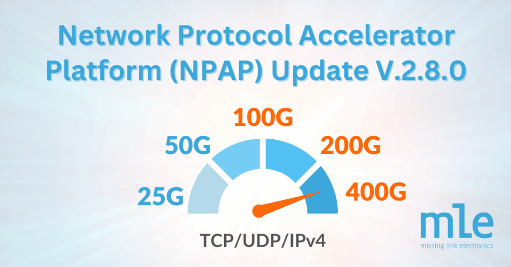
NPAP is the TCP/UDP/IP Full Accelerator from Fraunhofer HHI which enjoys production use in FPGA applications for automotive, industrial, medical, robotics, test & measurement and wired/wireless communications.