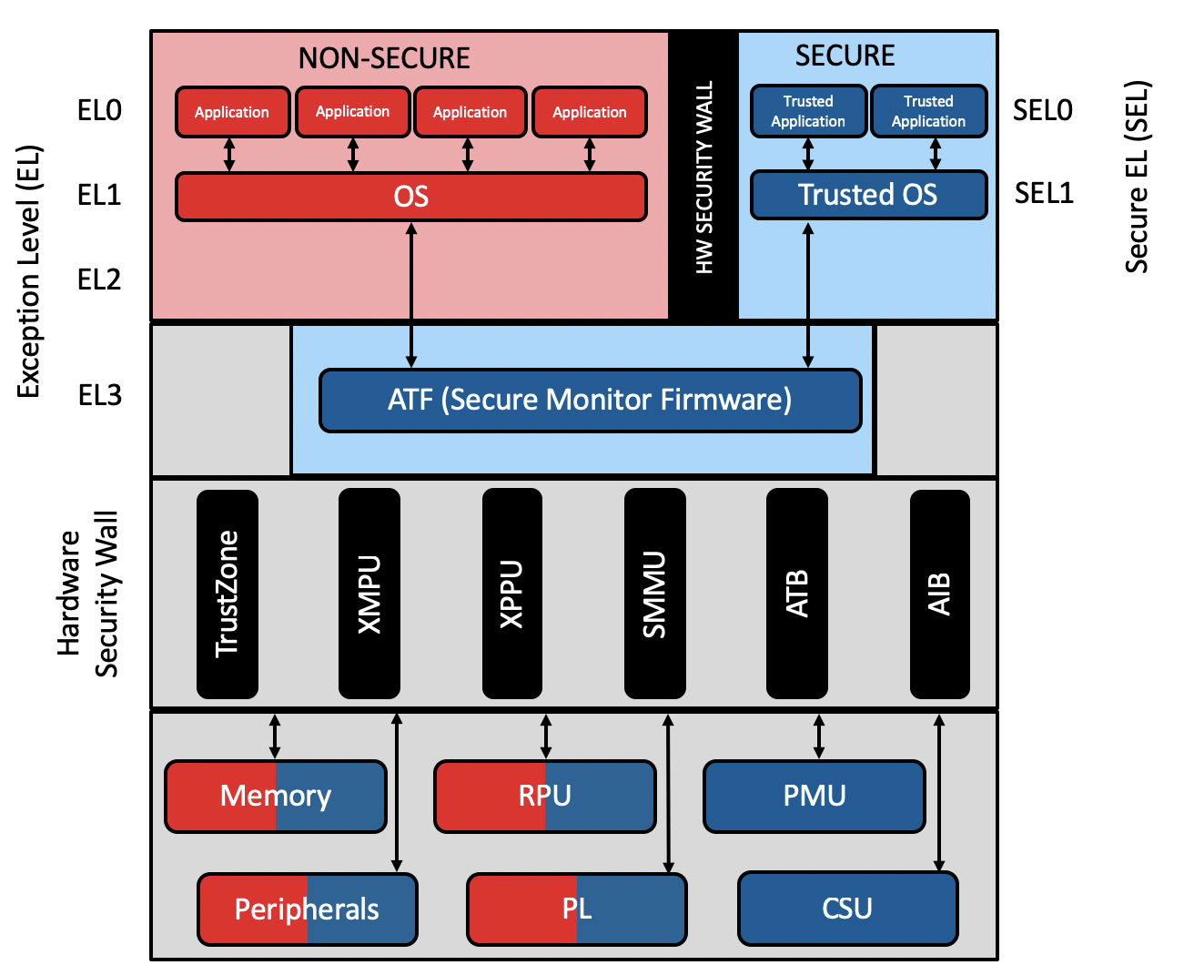
Auto/TSN
Auto/TSN
In-Vehicle Network - Auto/TSN
Auto/TSN stands for automotive data over Time-Sensitive Networks which is an in-vehicle network infrastructure based on open standards such as IEEE Ethernet. Auto/TSN is the results of a collaborative effort between MLE and MLE partners, Fraunhofer HHI and Fraunhofer IPMS.
Fundamentally, Auto/TSN virtualizes the in-vehicle network infrastructure: Key objective is to reduce costs, increase scalability and enable upgradability for next-generation automotive architectures including electric and/or autonomous vehicles.

By tunneling sensor data along with PCIe and NVMe over Real-Time Multi-Gigabit Automotive Ethernet Auto/TSN simplifies the wire harness and enables more centralized architectures with higher levels of hardware / software integration. By offering PCIe as a common interface (for sensor-to-CPU and CPU-to-CPU connectivity) Auto/TSN different semiconductor SoCs become interchangeable. This significantly reduces semiconductor dependencies and infrastructure costs at the same time.
Auto/TSN is highly scalable and supports line-rates up to 50 Gbps in FPGA and 100 Gbps in ASIC. Based on IPv4, the space for addressing nodes is 32 bits wide. The small hardware footprint allows zonal gateways with many ports.
Auto/TSN is “software-defined” and builds from open standards such as IEEE 802.1Q TSN, IEEE 802.3 Ethernet, IETF TCP/IP, MIPI CSI-2, PCIe 4.0 and NVMe 1.4 and open-source Linux which eases hardware / software / system upgradability.
Features & Benefits of In-Vehicle Network Auto/TSN
Auto/TSN is a network infrastructure with a system/software focus which reduces the complexity of connecting sensors and centralized computers because it follows de-facto standards of open source network APIs such as RDMA, Linux netdev or SOME/IP.
Benefits include:
- Significant cost-down for in-vehicle networking and wire harnesses
- Digital cicruit implementation for zero CPU load
- Deterministic and very low transport latencies, typ. within 5 micro-seconds
- Low footprint enables ASIC or FPGA implementation
The current implementation of TSN supports time-synchronization (IEEE 802.1AS) with 20 nanosecond precision, traffic shaping (IEEE 802.1Qav, 802.1Qbv), frame replication (IEEE 802.1CB) and stream prioritization (IEEE 802.1Qat) for high reliability, low-cost redundancy for functional safety and real-time behavior. Because for PCIe “best effort” is not sufficient, Auto/TSN implements a reliable transport on top of TSN which is compliant to IETF TCP/IP.
For in-vehicle network security Auto/TSN can be complemented with state-of-the-art IEEE 802.1AE MAC Security Entities (MACsec) and/or IETF RFC 6071 Internet Protocol Security (IPsec) and/or IETF RFC8446 Transport Layer Security (TLS).
Various Connectivity Schemes are supported:
- Single CPU (PCIe Root-Port) to multiple devices (PCIe Endpoints)
- Single CPU to multiple SSDs via NVM Express (NVMe)
- Multiple CPUIs to multiple NVMe SSDs (via NVMe proxy)
- Multiple CPUs to multiple CPUs via Inter-System Bridge (a.k.a. PCIe NTB)
- Asymmetric sensor connectivity, e.g. MIPI CSI-2 to PCIe
- IEEE 1722 style video transport

Data-in-motion processing runs on dedicated on-chip full accelerators and frees up the CPUs from protocol handling. Our patented and patent-pending Heterogeneous Packet-Based Transport mechanism packetizes and de-packetizes PCIe, MIPI CSI-2 and other packet-based protocols and features low protocol overhead for high bandwidth and low and deterministic micro-second transport latency.
PCIe Over Auto/TSN
Auto/TSN implements a PCIe switch compliant with PCI-SIG Base Specification 3.0 (or newer) and NVM Express Specification 1.2 (or newer).
PCIe Inter-System-Bridge for Auto/TSN
Integrated PCIe Inter-System Bridges (a.k.a Non Transparent Bridges / NTB) enable CPU-to-CPU connectivity. The PCIe Inter-System Bridges use a least-cost write-only protocol to deliver very high read/write performance. This allows direct connectivity between sensors and multiple CPUs, GPUs, FPGA, SoCs, peripherals and next-generation storage within the entire vehicle.
MIPI CSI-2 Over Auto/TSN
Image sensors can connect via standard MIPI D-PHY and MIPI CSI-2, or else. Multicast functionality transports data from each image sensor to one, or more, central compute units under real-time conditions. Hence, Auto/TSN allows symmetric (e.g. PCIe-to-PCIe) and asymmetric (e.g. MIPI CSI-2-to-PCIe) communication schemes.
IEEE 1722 Video Transport Over Auto/TSN
Complementing the MIPI CSI-2 over Auto/TSN transport, MLE has also implemented a solution that follows the Raw Video PDU Format from IEEE 1722.Similarly, this IEEE 1722 Raw PDU Transport supports point-to-point connectivity or multicast where one sensor's image data can be sent to multiple CPUs simultaneously.
Availability
Auto/TSN is available as a licensable integrated subsystem stack comprising digital circuit implementations and device driver software. This business model gives OEMs and Tier1s full control over how to integrate, either as a dedicated semiconductor component, or as modular function blocks inside a custom System-on-Chip with additional customer-specified functionality.
MLE has been working with key semiconductor partners to deliver FPGA and ASIC based implementations of Auto/TSN ready for design and for production. Our early access program supports OEMs and Tier1s to perform in-house benchmarking and validation of Auto/TSN.
Current implementations support gateway nodes with PCIe 3.0 and NVMe 1.2 with up to 4 lanes and with 5 or 8 GT/s, MIPI D-PHY 2.0 with up to 4 lanes and 2 Gbps and MIPI CSI-2 2.0 and up to 8 1G/10G Ethernet ports over copper or over fiber. “Lab Cars” based on professional 3rd party ASIC hardware emulators are available upon request.

Documentation
- PCIe Range Extension via Robust, Long Reach Protocol Tunnels (presented at PCI-SIG Developers Conference 2018)
- Sensor Fusion and Data-in-Motion Processing for Autonomous Vehicles (presented at PCI-SIG Developers Conference 2019)
- PCIe-over-TCP-over-TSN-over-10/25 GigE (presented at the FPGA-for-ADAS Workshop 2020)
- Zone-Based Automotive Backbones Tunneling PCIe (presented at PCI-SIG Developers Conference 2021)
Fraunhofer Heinrich-Hertz Institute
Founded in 1949, the German Fraunhofer-Gesellschaft undertakes applied research of direct utility to private and public enterprise and of wide benefit to society. With a workforce of over 23,000, the Fraunhofer-Gesellschaft is Europe’s biggest organization for applied research, and currently operates a total of 67 institutes and research units. The organization’s core task is to carry out research of practical utility in close cooperation with its customers from industry and the public sector.
Fraunhofer HHI was founded in 1928 as “Heinrich-Hertz-Institut für Schwingungs- forschung“ and joined in 2003 the Fraunhofer-Gesellschaft as the “Fraunhofer Institute for Telecommunications, Heinrich-Hertz-Institut„. Today it is the leading research institute for networking and telecommunications technology, “Driving the Gigabit Society” .
Fraunhofer Institute for Photonic Microsystems
Fraunhofer IPMS is a worldwide leader in research and development services for electronic and photonic microsystems in the fields of Smart Industrial Solutions, Medical & Health applications and Improved Quality of Life. Innovative products can be found in all large markets – such as ICT, consumer products, automobile technology, semiconductor technology, measurement and medical technology – products which are based upon various technology developed at Fraunhofer IPMS.
Security & Trust

Security & Trust
OP-TEE: Open-Source Secure Operating System
OP-TEE: Open Portable Trusted Execution Environment OP-TEE is a small secure operating system which, after authentication and decryption, gets loaded in an secured area in the memory. A Rich OS (e. g. Xilinx PetaLinunx) driver can request, via a Secure Monitor Call, the execution of a trusted application.
OP-TEE is an Open-Source initiative driven by a Linaro team who maintains the code and makes it available for download at GitHub.
MLE took the effort to port OP-TEE to Xilinx Zynq UltraScale+ MPSoC and RFSoC devices and included device specific optimizations. The outcome is two-fold: Tightly integrated Open-Source maintained by experts of Xilinx System-on-Chip and ACAP technology. And, additional professional services for customization and product life cycle support.
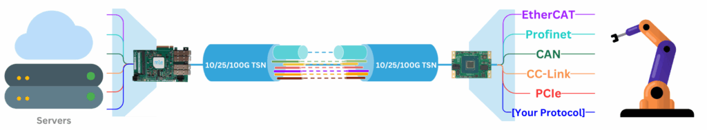
Key Features of OP-TEE in FPGAs
- Enables running secure & trusted applications from within a rich Linux operating system
- Utilizes standard ARM Trusted Execution Environment (TEE)
- Utilizes advanced security functions in Xilinx Zynq UltraScale+ MPSoC and RFSoC devices
- Optional hardware acceleration for AES-CGM, RSA, SHA3, etc
- Optional secure key handling with integrated PUF (Physically Unclonable Function) support
- Optional handling for integrated eFUSE burning
- Secure and non-secure bitstream loading
- Support for custom secure functions in Programmable Logic

Applications
- Secure data storage
- Secure communication
- Secure Over-the-Air (SOTA) updates
- Key to meet compliance with standards such as IEC 62443, IEC 27001 etc
- Protect Functional Safety (SIL, ASIL) related designs
- Secure touch inputs
- Secure key handling
Pricing
MLE OP-TEE is available as pure Open-Source or as a professionally maintained source code deliverable:
Product Name | Deliverables | Pricing |
---|---|---|
OP-TEE Open-Source Edition |
Licensed under BSD / Linaro terms and available for download from GitHub. |
Free of charge |
OP-TEE Professional Edition |
MLE Single-Site or Multi-Site Source Code License. Delivered by MLE in electronic form. | Annual subscription fees starting at $42,800.- |
Application / Project specific Expert Design Services |
System-level design, modeling, implementation and test for realizing Domain-Specific Secure appplications. | $1,480.- per engineering day |
OP-TEE Free
(Open Source Edition)
The OP-TEE Open Source Edition for Zynq UltraScale+ MPSoC and RFSoC is licensed under Linaro / BSD license as Open Source and comes with all source code and necessary packages. This version is ideal to explore the TEE world and develop your own trusted application.
Key Features and Benefits:
- Open Source and Free of Charge
- Runs in external PS-attached DDR memory
- No Hardware acceleration for AES, RSA, SHA3
- No access to PUF
OP-TEE PRO
(Professional Edition)
MLE OP-TEE PRO can be licensed from MLE and will provide all source code and necessary packages to run OP-TEE on Zynq UltraScale+ MPSoC and RFSoC.
Key Features and Benefits:
- Hardware acceleration for AES
- Hardware acceleration for RSA
- Hardware acceleration for SHA3
- With secure boot: access to PUF (Physical Uncloneable Function) functionality
- Can load OP-TEE into TCM
Comparison Between OP-TEE Free And OP-TEE PRO
Functionality Supported
OP-TEE Free
OP-TEE PRO
(extended)
Documentation
- Security / Trusted Execution Environment and Functional Safety with Zync Ultrascale+ MPSoC / RFSoC (presentation at the 3rd Workshop “Programmable Processing for the Autonmous / Connected Vehicle 2019”)
- OP-TEE online documentation
- OP-TEE Security Advisories
- Developer Services for Security from Linaro
- Xilinx Security Website (including presentations by MLE, available under NDA only)
- Whitepaper 513 from Xilinx on IEC 62443 Compliant Product Enablement
Frequently Asked Questions
What is the difference between MLE OP-TEE PRO and the open source edition?
Most of the Zynq UltraScale+ MPSoC / RFSoC (ZynqMP) specific code for OP-TEE is currently going upstream to become part of the free open-source edition.
However, there are functions of ZynqMP which require special handling, like the one-time-programmable eFuses, or support for custom secure PL functions, for example. Such device and/or application specific security functions of ZynqMP will be covered only by the PRO edition. Please refer to the comparison table above.
Is source code for OP-TEE PRO available?
Yes, MLE ships source code for OP-TEE PRO. Those ZynqMP platform specific code portions are available today and have passed review by the Xilinx Security Center of Excellence (COE). The most recent review was November 2019.
What is the cost of OP-TEE Free?
OP-TEE Free is free-of-charge open-source software (FOSS) and can be downloaded from here: https://github.com/OP-TEE/ under a BSD 2-Clause License.
What is the cost of OP-TEE PRO?
Please refer to the Pricing section above.
Function Accelerators

Network Function Accelerators, FACs, NICs and SmartNICs
Deterministic Networking: NICs, SmartNICs, and Function Accelerator Cards
A Network Interface Card (NIC) is a component which connects computers via networks, these days mostly via IEEE Ethernet – but what makes a NIC a SmartNIC?
With the push for Software-Defined Networking, (mostly open source) software running on standard server CPUs became a more flexible and cost-effective alternative to custom networking silicon and appliances. However, in the post Dennard scaling area, server CPU performance improvements cannot keep up with increasing computational demand of faster network port speeds.
This widening performance gap creates the need for so-called SmartNICs. SmartNIC not only implement Domain-Specific Architecture for network processing but also offload host CPUs from running portions of the network processing stack and, thereby, free up CPU cores to run the “real” application.
According to Gartner, Function Accelerator Cards (FACs) incorporate functions on the NIC that would have been done on dedicated network appliances. Hence, all FACs are essentially NICs, but not all NICs/SmartNICs are FACs. When deployed properly, FACs can increase bandwidth performance, can reduce transport latencies and can improve compute efficiency, which translates to less energy consumption.

Features of Functional Accelerators
Ultra-Reliable, Low-Latency, Deterministic Networking
With ultra-reliable, low-latency, deterministic networking we have borrowed a concept from 5G wireless communication (5G URLLC) and have applied this to LAN (Local Area Network) and WAN (Wide Area Network) wired communication:
- Ultra-Reliable means no packets get lost in transport
- Low-Latency means that packets get processed by a FAC at a fraction of CPU processing times
- Deterministic means that there is an upper bound for transport and for processing latency
We do this by combining the TCP protocol, fully accelerated (in FPGA or ASIC using NPAP), with TSN (Time Sensitive Networking) optimized for stream processing at data rates of 10/25/50/100 Gbps. These so-called TCP-TSN-Cores not only give us precise time synchronization but also traffic shaping, traffic scheduling and stream reservation with priorities.
We believe that FPGAs are very well positioned as programmable compute engines for network processing because FPGAs can implement “stream processing” more efficiently than CPUs or GPUs can do. In particular, when the networking data stays local to the FPGA fabric Data-in-Motion processing can be done within 100s of clock cycles (which is 100s of nano-seconds) and can be sent back a few 100 clock cycles later, an aspect with is referred to as Full-Accelerated In-Network Compute.
While FPGA technology has been on the forefront of Moore’s Law and modern devices such as AMD/Xilinx Versal Prime or Intel Agilex or Achronix Speedster7t can hold millions of gates, FPGA processing resources must be used wisely, when Bill-of-Materials costs are important. Therefore, at MLE we have put together a unique combination of FPGA and open-source software to achieve best-in-class performance while addressing cost metrics more in-line with CPU-based SmartNICs.
Unique and Cost-Efficient Combination of Open Source
The Open Source Technologies We Borrow From
Linux kernel
Meanwhile highly optimized for networking
OpenvSwitch
An open source multi-layer network switch
Intel Compiler for SystemC
An open source High-Level Synthesis engine
OpenNIC
The GitHub project focusing on AMD/Xilinx Alveo cards
Xilinx Vitis HLS LLVM
The High-Level Synthesis Frontend for Xilinx FPGAs
High-Level Synthesis plays a vital role in our implementation as it allows MLE and MLE customers to turn algorithms implemented in C/C++/SystemC into efficient FPGA logic which is portable between different FPGA vendors.
To build a high-performance FAC platform, portions of the above have been integrated together with proven 3rd party networking technologies:
- NPAP, the Network Protocol Accelerator Platform which is a TCP/UDP/IP Full Accelerator that comes from Fraunhofer HHI
- TSN, which is Time Sensitive Networking, a collection of IEEE Standards implemented by Fraunhofer IPMS
Corundum In-Network Compute + TCP Full Accelerator
Corundum is an open-source FPGA-based NIC which features a high-performance datapath between multiple 10/25/50/100 Gigabit Ethernet ports and the PCIe link to the host CPU. Corundum has several unique architectural features: For example, transmit, receive, completion, and event queue states are stored efficiently in block RAM or ultra RAM, enabling support for thousands of individually-controllable queues.
MLE is a contributor to the Corundum project. Please visit our Developer Zone for services and downloads for Corundum full system stacks pre-built for various in-house and off-the-shelf FPGA boards.
MLE combines the Corundum NIC with NPAP, the TCP/UDP/IP Full Accelerator from Fraunhofer HHI, via a so-called TCP Bypass which minimizes processing latency of network packets: Each packet gets processed in parallel by the Corundum NIC and by NPAP. The moment it can be determined that the packet shall be handled by NPAP (based on IP address and port number) this packet gets invalidated inside the Corundum NIC. If a packet shall not be processed by NPAP, it get’s dropped in NPAP and will solely be processed by the Corundum NIC.
Fundamentally, this implements network protocol processing in multiple stages: Network data which is latency sensitive does get processed using full acceleration, while all other network traffic is handled either by a companion CPU and/or by the host CPU.
Applications of Function Accelerators
MLE’s Function Accelerators are of particular value where network bandwidth and latency constraints are key:
- Wired and Wireless Networking
- Acceleration of Software-Defined Wide Area Networks (SD-WAN)
- Video Conferencing
- Online Gaming
- Industrial Internet-of-Things (IIoT)
- Handling of Application Oriented Network Services
- Mobile 5G User-Plane Function Acceleration
- Mobile 5G URLLC Core Network Processing with TSN
- Offloading OpenvSwitch (OvS), vRouter, etc
Key Benefits
The following shows the key benefits of MLE’s technology by comparing open-source SD-WAN switching in native CPU software mode against MLE’s Ultra-Reliable Low-Latency Deterministic Networking:
![]() |
![]() |
Compared with plain CPU software processing MLE’s Ultra-Reliable Low-Latency Deterministic Networking increases network bandwidth and throughput close to Ethernet line rates, in particular for smaller packets, which reduces the need for over-provisioning within the backbone. And, processing latencies can be shortened significantly which is important, for example, when delivering a lively audio/video conferencing experience over WAN.
Availability
MLE’s Ultra-Reliable Low-Latency Deterministic Networking is available as a licensable full system stack and delivered as an integrated hardware/firmware/software solution. In close collaboration with partners in the FPGA ecosystem, MLE has ported and tested variations of the stack on a growing list of FPGA cards. Currently, this list comprises high-performance 3rd party hardware as well as MLE-designed cost-optimized hardware:
FPGA Card |
Hardware Description & Features |
Status |
![]() |
NPAC-Ketch, MLE-designed single-slot FHHL PCIe card
|
Available Inquire |
![]() |
FALCON 1SM21, prodesign designed FHFL PCIe card
|
Early Access |
![]() |
HAWK VC1902, prodesign designed FHFL PCIe card
|
Early Access |
![]() |
Sidewinder-100, Fidus Systems designed single-slot FHFL PCIe card
|
Available |
![]() |
Alveo U280, AMD/Xilinx-designed dual-slot FHFL PCIe card
|
Early Access |
![]() |
N6000-PL, Intel-designed single-slot FHHL PCIe card
|
Early Access |
Documentation
- Ultra-Reliable, Low-Latency, Deterministic Networking
- Function Accelerator Card – NPAC-40G
- MLE Technical Brief – MLE-TB20201203 “Deterministic Networking with TCP-TSN-Cores for 10/25/50/100 Gigabit Ethernet”(MLE-TB20201203)
Solutions
Solutions
Network Acceleration and Security Solutions
Nowadays the demands in high-bandwidth, low-latency networking and storage increase day by day. MLE leverages FPGAs to offload CPUs and accelerate software-rich system stacks for In-vehicle Networking, Smart Network Interface Cards (Smart NICs), FPGA-based Acceleration, and the secure solution OP-TEE compatible with FPGA.
In-Vehicle Networking
In-Vehicle Networking for Zone-based automotive architectures requires high data rate and real-time behavior. Auto/TSN builds on top of MLE’s patented and patent pending technology, integrates technology from MLE partners Fraunhofer and CERN, and follows open standards IEEE Time-Sensitive Networking, PCI-SIG PCIe Express, and IETF TCP/UDP/IP.
Smart NICs
MLE provides full system stacks for FACs (Function Accelerator Cards) and Smart NICs (Network Interface Cards) for wired and wireless communications. This unique combination of connectivity technology from Fraunhofer plus MLE’s patented and patent-pending Full Accelerators accelerates Software-Defined Networking (SDN).
Security and Trust
MLE provides solutions to secure products based on FPGA technology: MLE has ported OP-TEE to AMD/Xilinx Zynq UltraScale+ MPSoC and RFSoC including support for black keys, PUFs, eFUSES, etc. Furthermore, MLE has introduced networking security products for deep packet inspection and Data Diodes.
FPGA-Based Acceleration
MLE provides platforms and middleware using various FPGA-based accelerator cards for applications running on ARM, RISC-V, x86, amd64, IBM OpenPOWER.